


Part 1 of this article discussed the similarities and differences between the well-known processor memory hierarchy and the FPGA memory hierarchy. Although similar, the FPGA memory hierarchy lacks the multiple cache levels now common in microprocessor design. Similarly, the processor hierarchy lacks some of the more specialized memory structures and interfaces developed to satisfy an FPGA’s unique memory needs. Part 2 discusses these specialized FPGA memories.
About a quarter of a century ago, the FPGA vendors started to add larger RAM blocks to the mix of on-chip memory resources in the FPGA memory hierarchy, shown in Figure 1 below (repeated from Part 1 of this article for your convenience).
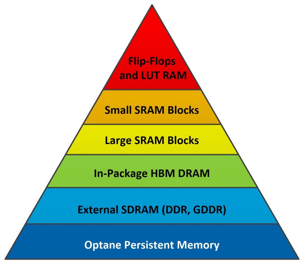
Figure 1. FPGA Memory Hierarchy
The first embedded SRAM blocks to appear showed up as 2Kbit “Embedded Array Blocks” in the Altera Flex 10K FPGAs, announced in 1995. From the perspective of designers using FPGAs, this was a killer new feature and Xilinx followed suit in 1998 when it announced the first-generation Virtex FPGAs.
Since those early days, embedded RAM blocks in FPGAs have grown. Today’s large FPGAs contain many Mbits worth of dual-ported Block SRAMs. Intel FPGAs now incorporate 20-Kbit M20K memory blocks. (Note: Intel bought Altera in 2015.) Xilinx initially dubbed its embedded SRAM blocks “SelectRAM” but now just calls them Block RAMs, which are 36-Kbit, dual-ported SRAM blocks. The Block RAMs on the Achronix Speedster7t FPGA are even larger, storing 72 Kbits each.
Of course, these larger block RAMs were not enough either. As system designers started using FPGAs for bigger and bigger designs, new FPGA applications began processing new, bigger data types such as images, audio streams, and video frames that demanded even more fast on-chip memory. At first, design engineers started to concatenate the relatively small M20K memory blocks and Block RAMs to make even larger memories. Soon everyone needed these larger memories. However, it makes little sense to force everyone to glue smaller block RAMs together using programmable logic. Again, the FPGA vendors responded.
In 2015, Xilinx introduced its Virtex UltraScale+ FPGAs 288-Kbit SRAM memory blocks, dubbed UltraRAM, to meet the need for much larger embedded memories. (The name “UltraRAM” calls to mind a particularly successful Japanese children’s TV show from the 1960s called “Ultraman” that featured a giant and very durable superhero dressed up in a red and silver rubber suit.) Similarly, Lattice has incorporated half-Mbit Large Random Access Memory (LRAM) blocks in its recently announced CertusPro-NX FPGA family. (See “Xilinx Throws Down, Unveils New 16nm UltraScale+ Families” and “Lattice Launches CertusPro-NX.”)
However, the big kahuna of large embedded SRAM blocks, at least for now, has to be the 18-Mbit and 47.5-Mbit embedded SRAM (eSRAM) blocks found in the latest Intel FPGAs. These eSRAM blocks are extremely configurable and are designed to be divided into several smaller SRAM blocks in your design. Currently, two members of the Intel Agilex FPGA family incorporate eSRAM blocks (with two 18-Mbit blocks per device) and ten members of the Intel Stratix 10 FPGA family incorporate eSRAM blocks (with two 47.25-Mbit blocks per device).
Need more speed? Go off chip
Eventually, these various on-chip FPGA memories proved insufficient to meet design requirements. When that happened, when designers needed many Mbytes or Gbytes of memory, off-chip memory became the initial next jump down the FPGA memory hierarchy. It’s relatively easy to connect external SRAM to FPGAs using conventional parallel I/O ports. No special memory controller is needed. However, DRAM presents a more complex design challenge. No one likes to design DRAM controllers, especially SDRAM controllers, from scratch. There are too many rules. There’s too much opportunity to make a design mistake. Consequently, FPGA vendors started to incorporate hardened, tested DRAM controllers into their devices.
These days, the memory controllers incorporated into FPGAs are designed to control various DRAM and SDRAM generations, which add many Gbytes of memory capacity to the FPGA memory hierarchy. However, going to off-chip memory and switching to DRAM or SDRAM means that this level in the FPGA memory hierarchy is much, much slower than the on-chip memories that reside higher up in the hierarchy. The latest FPGAs support DDR5 SDRAM DIMMs, which currently can operate at peak data-transfer rates as fast as 51.2 GBytes/sec, per DIMM. The older and more common DDR4 SDRAM DIMMs top out at 32 Gbytes/sec per DIMM for the fastest speed grade, DDR4-4000.
For applications where external DDR SDRAM is too slow, performance-oriented GDDR SDRAM is a possible but more expensive alternative, used only when external memory subsystem performance is more important than the cost per bit of storage. The GDDR interface differs from the DDR4 or DDR5 interface, so only certain FPGAs have been designed to be mated with GDDR SDRAM, which is most commonly used with GPUs – after all, the “G” in GDDR stands for “graphics.”
At least one FPGA memory controller supports GDDR SDRAM. Specifically, the Achronix Speedster7t FPGA family is designed to control as many as eight GDDR6 SDRAM banks. Each GDDR6 interface port on a Speedster7t FPGA can support transfer rates as fast as 64 Gbytes/sec for an aggregate memory bandwidth of 512 Gbytes/sec when all eight of the GDDR memory ports on an Achronix Speedster7t1500 FPGA are used. The Bittware S7t-VG6 VectorPath Accelerator Card is an example of a high-performance PCIe accelerator that pairs an Achronix Speedster7t FPGA with GDDR6 (and DDR4) SDRAM.
(Note: In July, SK Hynix announced that it had just started mass producing LPDDR4-4266 SDRAM, which is half as fast as the equivalent DDR4 module in terms of Gbytes/sec, thanks to having half the data bus width. The company also said it plans to use the same process technology node to make DDR5 SDRAM next year. When that happens, it will likely raise the ceiling on DDR5 SDRAM transfer rates and shrink the gap between DDR5 and GDDR6 SDRAM even further, but that doesn’t mean that FPGA memory controllers compatible with DDR5 SDRAM will automatically be able to go just as fast.)
Need even more speed? Go back inside the package
External DRAM in the form of DDR or GDDR SDRAM leaves a significant gap between the capacity and performance of an FPGA’s on-chip SRAM and off-chip SDRAM. That gap is now filled with High-Bandwidth Memory (HBM) modules, which are 3D stacks of DRAM (not SDRAM) die that couple to the FPGA die inside of the FPGA package using 3D semiconductor packaging techniques. Each HBM die stack connects to the FPGA die through a fast, massively parallel, 1024-bit bus. Current examples of FPGAs that incorporate HBM are the Intel Stratix 10 MX and Stratix 10 NX device families and Xilinx Virtex UltraScale+ HBM devices.
HBM adds 8 to 16 Gbytes of memory capacity to the FPGA, for a price. HBM is larger and slower than the FPGA’s on-chip SRAM resources but faster than off-chip SDRAM, albeit with lower maximum capacity than SDRAM and with higher cost per bit. Because of the massively parallel interface and short in-package interconnect, HBM delivers much higher data rates compared to SDRAM. For example, second-generation HBM2 can deliver 256 GBytes/sec of peak memory bandwidth per DRAM stack. SK Hynix claims that HBM2E can achieve 460 GBytes/sec per stack and that HBM3 stacks, currently under development, will hit 665 Gbytes/sec. So basically, we’re talking an order of magnitude faster than DDR4 or DDR5 here. Of course, you’ll never hit these projected peak bandwidth specs in real life. (Remember, you’ve been warned.)
Vendors offer a few FPGA families with in-package HBM, including the Intel Stratix 10 MX and Stratix 10 NX FPGAs and the Xilinx Virtex UltraScale+ HBM family. Xilinx recently added the Versal HBM FPGA family to its list. The Intel Web site lists an Agilex M-series FPGA family that incorporates HBM with the phrase “Coming Soon” attached to the listing. These FPGA families with integrated HBM DRAM stacks are for applications requiring the absolute maximum performance offered by the FPGA vendors. HBM showed up on FPGAs far later than embedded DRAM controllers, and this 3D stacked-die technology is an example of a newer memory technology burrowing into the middle of the existing memory hierarchy to fill a specific need – the need for speed.
There’s Something About Optane
Nonvolatile Intel Optane PMem (Persistent Memory), discussed in Part 1 of this article, provides another example of a new memory technology that has been added to the FPGA memory hierarchy to fill a need: high-capacity, nonvolatile memory. Optane PMem DIMMs look a lot like SDRAM with respect to the physical interface, but the timing’s a little different and there’s no need for refresh cycles. Intel coaxed the on-chip SDRAM memory controllers on its Intel Stratix 10 DX FPGAs to work with Intel Optane PMem with a little tweaking. At this time, only Intel FPGAs are designed to work with Intel Optane PMem, which is slower than SDRAM but delivers more storage capacity with nonvolatility, so it sits very nicely below SDRAM on the FPGA memory hierarchy, as shown in Figure 1 above.
Where does all this leave you as a system designer? If you’re designing with FPGAs, you have more memory choices at different price/performance points than at any earlier time in the FPGA’s 35-year history. Unless you need some of the more exotic memory forms such as HBM, GDDR6, or UltraRAM, your choices remain wide open, because all of the FPGA vendors have leveraged each other’s best ideas and now offer several different levels in the memory hierarchy in most of their device offerings. That means that other factors such as total available resources, power consumption, product availability, unit cost, or a preference for one vendor’s development tools over the others are more likely to sway your choices.
Still, it’s nice to have choices, isn’t it? Feel free to discuss your experiences with the FPGA memory hierarchy in the comments below. I’d love to hear about them.


