


One simplistic way to think about FPGA anatomy is to split everything inside of the FPGA into two categories: resources that do stuff (process bits) and resources that remember stuff (store bits). The resources that do stuff include the programmable logic, the DSP slices, embedded math blocks, and even the serial transceiver ports. The resources that store stuff include the flip-flops embedded in the programmable logic blocks, LUT RAM, big and little embedded SRAM blocks, and on-chip HBM DRAM. There’s also the special case of the extra memory chips you attach to the FPGA, which might be larger SRAMs, SDRAMs, and – in Intel’s case – Optane PM (Persistent Memory). How much of each kind of memory your design needs depends heavily on your application, so it’s a very good idea to understand what each type of memory can do, and what it costs.
There’s a classical way to think about memory and storage for microprocessors called “The Memory Hierarchy,” shown in Figure 1.
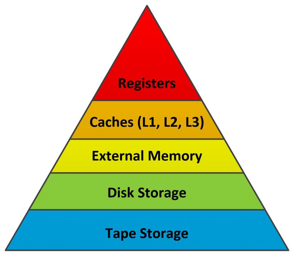
Fig 1. Classical Processor Memory Hierarchy
The memory hierarchy is drawn as a triangle to represent how much of each memory type you get in typical systems. The CPU and its registers sit at the triangle’s apex. Registers run at computational speed. Because they’re fast and intimately connected to the computational hardware, they also need to be relatively small and store the fewest number of bits.
Caches sit just below the CPU registers in the processor memory hierarchy. They’re not as fast as CPU registers, because they’re big, but because they’re built with SRAM, they’re still pretty fast. The earliest microprocessors had no cache. Processor clock rates were slow – just 1, 2, or 4 MHz – and external SRAM memory could keep pace with the processor. Sometimes, even DRAM could keep up. However, when processing speeds started to climb, the processors’ thirst for instructions and data outstripped external memory’s ability to supply that data, so processor architects started to add on-chip caches.
Initially, only one level of cache was needed. Then two. Then three. I find it useful to think of caches as being similar to automatic transmissions in cars. As you shift through the gears, the car goes faster but there’s less torque. As you sift through cache levels, the caches get bigger and slower. That’s in the nature of cache design and physics. As caches get bigger, they get slower. The cache-level hierarchy just falls out of that situation naturally.
Main memory sits below the caches. In very early microprocessor systems, main-memory capacity was likely to be only a few kilobytes and made of SRAM. Software developers quickly needed more and more main memory as programs grew and as processors started handling larger data objects: first images, then audio, then video, then multiple video streams. Larger memory requirements necessitated the substitution of DRAM for SRAM, chiefly for economics. DRAM is much less expensive per bit (good) but much slower (bad). The advent of relatively slow DRAM as bulk processor memory was just as much a factor in the development of on-chip caches as was rising processor speeds.
Storage in the form of disk and tape drives sits below main memory in the processor memory hierarchy. These are very interesting topics all by themselves, but they’re not relevant to a discussion of FPGA memory, so we’ll leave the disk and tape discussions for a later date.
The Official Memory Guy Memory Hierarchy
My good friend Jim Handy, who bills himself as “The Memory Guy,” has a different and very handy (pun intended) way to think about the memory hierarchy for processors that includes some actual numbers for price and bandwidth, shown in Figure 2.
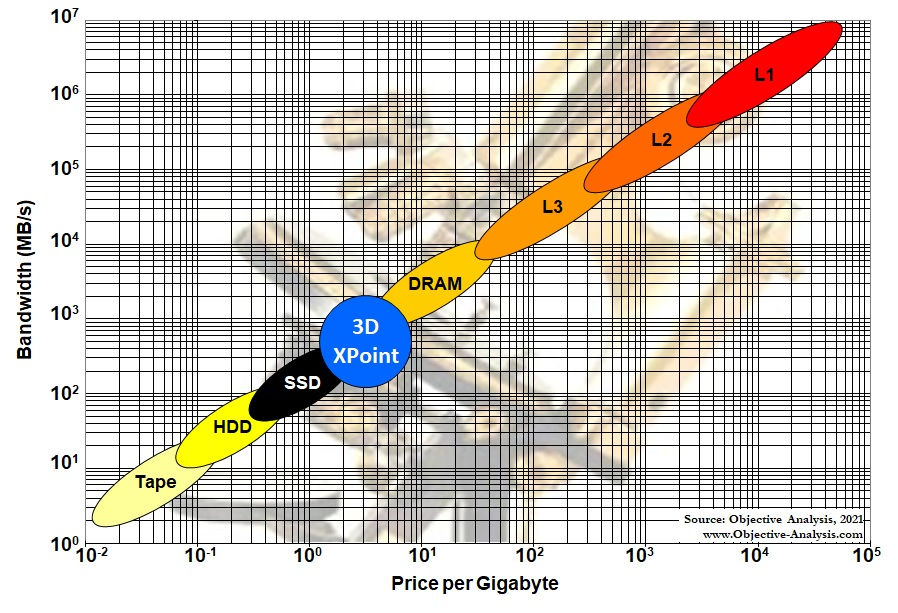
Fig 2. The Memory Guy’s Memory Hierarchy for Processors
(Used with permission.)
The Memory Guy’s hierarchy shows the different types of memory on a log-log chart with price per Gbyte plotted along the X axis and bandwidth plotted along the Y axis. This chart helps you to visualize why system designers use so many different memory types. It’s because computation must use a divide-and-conquer approach to solving problems. Processors can only process so much at one time, and the “much” that they can process must fit inside the processor’s registers (shown in the general hierarchy of Figure 1 but not in The Memory Guy’s hierarchy in Figure 2). As you move down the hierarchies, larger memories hold more, cost less per bit, and have lower data-transfer rates.
A second reason for showing The Memory Guy’s hierarchy is the blue circle labeled “3D XPoint” in the middle of the hierarchy. 3D XPoint memory is a relatively new, nonvolatile memory that was a years-long joint development project between Intel and Micron. Intel has branded 3D XPoint memory products as “Optane,” and Micron… well Micron never quite commercialized it successfully.
Earlier this year, Micron announced that it was dropping 3D XPoint. In July, Micron announced that Texas Instruments (TI) was buying the one and only 3D XPoint production fab, located in Lehi, Utah. It does not appear that TI will be using this fab to make 3D XPoint devices. TI apparently plans to repurpose the fab for its own products – imagine that – which leaves Intel with the problem of figuring out how to make Optane memory in the future. But that’s a different story for another time. For now, you need to know that Intel isn’t likely to drop its support for Optane memory, because it’s an important part of the Intel Xeon CPU story and a point of differentiation for Intel’s server processors. Intel Optane PMem can also be in an FPGA’s memory hierarchy, as long as it’s an Intel FPGA (for now, anyway).
The FPGA Memory Hierarchy
Intel introduced the first commercial microprocessor, the 4-bit 4004, in November, 1971. Xilinx announced the first FPGA exactly 14 years later, in November, 1985. During that time, microprocessors had evolved quite a bit as had the processor memory hierarchy. Caches appeared. DRAM became the principle technology for a microprocessor’s main memory. Hard drives became practical as microprocessor peripherals.
FPGAs are not processors, but they do use memory for storage, so there were plenty of reasons to adapt bits and pieces of the processor memory hierarchy as FPGAs evolved. The first FPGA, the Xilinx XC2064, had an array of logic cells and nothing more, so the only memory in this first device were the flip-flops inside of the logic cells. Those earliest FPGAs had no memory hierarchy, or rather they had a 1-level hierarchy with just one kind of memory: flip-flops in the programmable logic cell. By the time Xilinx announced its XC4000 FPGA series in 1991, six years later, it had figured out how to repurpose the logic cell’s configuration RAM as a 16-bit distributed SRAM or “LUT RAM” to make it available for systems design.
As FPGAs evolved, so did the FPGA memory hierarchy. FPGA sales volumes are much smaller than sales volumes for microprocessors, so FPGA-based designs tend to use the same sorts of memory devices developed for use with microprocessors. Today, there are a variety of different memory devices available for use with FPGAs, which have a somewhat different memory hierarchy as shown in Figure 3.
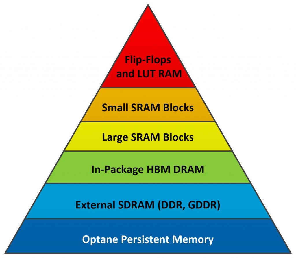
Figure 3. FPGA Memory Hierarchy
Flip-flops and LUT RAM embedded within the programmable logic blocks are the fastest and smallest memories incorporated into FPGAs. Along with accumulators built into FPGA DSP slices, these memories sit at the top of the FPGA memory hierarchy. They’re distributed throughout the FPGA’s programmable logic fabric, so there’s never a routing problem, but they’re very small – only a few bits each.
Designers quickly outstripped the capabilities of these smaller distributed FPGA memories and wished for more. The FPGA vendors granted their wishes through an evolutionary process, competitively driving each other to bigger and bigger on-chip RAM structures and memory controllers for large off-chip memory arrays as discussed in Part 2 of this article. Watch for it.
(Side Note: There’s another type of memory that’s critical for use with RAM-based FPGAs, and that’s the nonvolatile Flash memory that’s generally used to store and provide the configuration data to the FPGA during power-on initialization. You can also build Flash memory controllers using FPGAs. However, configuration memory and Flash controllers are not on-topic for a discussion of memory hierarchy, and I’m not going to discuss them here.)
Feel free to discuss your experiences with the FPGA memory hierarchy in the comments below. I’d love to hear about them.


Hi, Steve. I am using 3 dual port memory blocks, a few hundred LUTs, multiplier, and a comparator to build a new kind of computer. Read 2 operands, operator, address of next operator, next operands address all in one cycle. And with hundreds of memory blocks available, there can be hundreds on an FPGA.
The Visual Studio and compiler are free/open source. Also Quartus for FPGA design is free. That is for hobbyists and open source developers.
It has a vague similarity to MS’s project catapult which put FPGAs in the data centers. The “Where’s the Beef” research article referred to a study comparing FPGAs to superscalar CPUs and concluded that FPGAs win because of no instruction fetch. That is probably part of it. Most likely because 3 levels of cache waste so much bandwidth and power is also a big part of it.
It is all off the shelf, compiler, debugger, FPGA, Quartus. Nobody cares because of the hype and out of order, super scalar, multicore, HDL, HLS, nonsense.
Yes indeed, there’s gold in those FPGA memories. That is if anyone ever gets back to real logic design.
Thanks for commenting, Karl. As someone who has worked for Achronix, Xilinx, and Intel, I can say definitively that “real logic design” is alive and well. It may not look that way because the number of software programmers outnumber VHDL and Verilog slingers by 100:1 or 1000:1, but it’s still happening.
I am a logic designer and only use the HDLs for HARDWARE DESIGN as they were intended. They are not suited at all for LOGIC DESIGN.
The only way to debug is to synthesize, simulate, then try to show waveforms to see what happened.
Synthesis is limited to “synthesizable” blocks. Modules can be instantiated, but must be connected manually with absolutely no help from HDL or any part of the “tool chain”.
You may remember “MyHdl” from the days of “All Programmable Planet” which used Python to design and simulate, then create HDL for synthesis. Then there are SystemC, SystemVerilog, Redwood EDA maker chip, HLS all trying to do what logic design tools should be doing and then creating HDL for build.
Much of the effort is to compute values(evaluate expressions) and so far results are not spectacular.
Redwood EDA is more focused on logic/computer design and uses System Verilog for build.
What are the software engineers using? Odds are that some are using C# based on the number C# distributions.
Visual Studio IDE is used for C# development, and the first order of business is to instantiate classes that are similar to Verilog modules and interconnect those objects. The connections may be Boolean or
arithmetic values. If the value is from a different class, then it is an input that can be accessed by a get accessor of the source class and is an input to this class, all done at build time. If a value is used by a different class, it is an output of the source class and an input of the using class.
It is not magic or difficult, but the HDLs refuse to do it and require synthesis which means that all the connecting has to be done manually. HDL is a pitiful excuse for a design tool. No wonder there are so few HDLers. The obvious alternative is to use a computer programmed by a software engineer.
So I am using C# VS. 3 true dual port memory blocks, a multiplier, a comparator, some LUTs for logic nets and ALU on an FPGA.