

As usual, I’m amazed by how fast and how far things have changed in my own lifetime. When I started my career in electronics and computers in 1980, we thought simple programmable logic devices (PLDs) were pretty darned cool, not least that their creators managed to wring so many acronyms out of the same small collection of letters (engineers are nothing if not lovers of acronyms — especially of the TLA (three-letter acronym) variety).
The original PLDs were programmable read-only memories (PROMs), which appeared on the scene in 1970. Although these were somewhat simple, everyone was too polite to mention it. Programmable logic arrays (PLAs) first became available circa 1975, and these were followed by programmable array logic (PAL) and generic array logic (GAL) devices in the late 1970s. Over time, in addition to using programmable fuses to configure these devices, electrically programmable versions, like EPROMs, and electrically erasable programmable flavors, like EEPROMs, became available.
In many respects, the early days of PLDs were the equivalent to the Dark Ages for design engineers. In the case of PLDs, for example, we sometimes started by writing a truth table of inputs and outputs using a pencil and paper. Alternatively, we might capture a flow-chart diagram or schematic circuit (using the same pencil and a new piece of paper), after which we used things like Boolean equations, De Morgan transformations, and Karnaugh maps to generate our truth table. Ultimately, we ended up with a tabular text file on a computer defining which fuses were to be blown in the PLD. We then fed this file into a device programmer to blow the fuses. Each device programmer had its own file format, so creating one of these text files required intimate knowledge of both the device’s internal architecture and the file format used by the device programmer. (Error checks? Don’t make me laugh!)
It wasn’t until the 1980s that we began to see tools that performed the grunt work for us, starting with a committee of the Joint Electron Device Engineering Council (JEDEC) proposing a standard file format for PLD programming. It wasn’t long before all of the device programmers were modified to accept this JEDEC file format. This was followed by the introduction of PALASM (PAL Assembler), ABEL (Advanced Boolean Expression Language), and CUPL (Common Universal Tool for Programmable Logic), all of which involved rudimentary hardware description languages (HDLs) coupled with software applications that could convert design descriptions in these languages into corresponding JEDEC files. Oh, the fun we had!
In 1984, Xilinx started talking about a new type of device called a field-programmable gate array (FPGA). Instead of blowing fuses, this device was to be programmed using SRAM configuration cells. The first such device, the XC2064, became available to the market in 1985. This device had an 8×8 array of configurable logic block (CLB) islands, each containing two 3-input look-up tables (LUTs), all in a “sea” of programmable interconnect.
The thing was that there were no FPGA design tools in the early days, so it was up to the designers to specify the contents of each LUT and how the CLBs were to be connected to each other (and to the device’s primary inputs/outputs), all of which was done by hand (back to the pencil and paper again).
Detractors of the early FPGAs were fond of pointing out that the timing for these devices was non-deterministic because there were so many ways to connect things together inside. This was unlike PLDs, which were highly deterministic, with input-to-output delays specified in the data book.
All of these problems faded away with the introduction of language-driven design (LDD) using HDLs like Verilog and VHDL in conjunction with logic synthesis engines. Now, all the designer needed to do — in addition to capturing the design in register transfer level (RTL) code — was to specify any timing constraints along the lines of “The delay from input A to output Y should not exceed xx nanoseconds: The delay from input B to…” and so on, leaving it up to the synthesis engine to “make it so.”
Over time, FPGAs grew in capacity and performance. Today’s larger FPGAs, for example, can contain millions of equivalent gates, which has led to ever-increasing problems with respect to creating the optimal placement of logic functions and the routing between them so as to maximize resource utilization while minimizing routing congestion. All of which leads us to the guys and gals at Plunify, where this company’s moniker is a combination of “PL” (programmable logic) and “unify.”
Plunify, which was founded by Harnhua Ng and Kirvy Teo in 2009, is only a small company, but they’ve established an oversized footprint (no pun intended) with hundreds of customers, including around 50 Enterprise-level companies.
Plunify’s “Jewel in the crown” is a tool called InTime, which “sits on top” of existing place-and-route (P&R) and synthesis tools from major FPGA vendors like Xilinx, Altera (now Intel), and Microchip Technology.
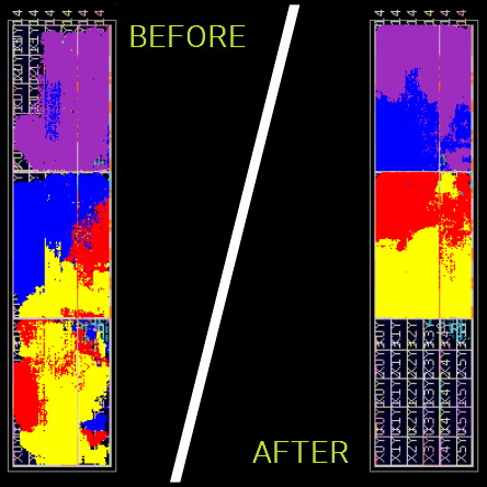
InTime analyzes the design’s RTL code but doesn’t modify it. Instead, it uses sophisticated machine learning algorithms to control the existing P&R and synthesis engines so as to realize optimal placement and routing, thereby achieve timing closure. It’s important to understand that P&R and synthesis tools have myriad control parameters that can be “tweaked.” Also, that everything is interrelated, so tweaking one parameter may improve one aspect of the design while negatively impacting another. The result is an extremely complex multivariate problem that is ideally suited to a machine learning solution. And, speaking of results, they are very impressive, as illustrated below:
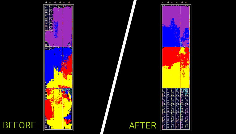
FPGA placement and routing “before” (using existing vendor tools) and “after” (augmenting those tools with InTime) (Image source: Plunify)
InTime, which is integrated with resource management software like LSF and SGE, works on a single machine or on multiple computers on a network, distributing builds and aggregating results across multiple machines automatically. Furthermore, Plunify Cloud allows you to offload builds to Amazon Web Services (AWS) without needing to be a cloud expert.
Now, although terms like “artificial intelligence” and “machine learning” may have a certain “buzz-word” cachet, users really don’t care one way or the other. All they are concerned about is whether the tool works or not and if it increases the quality of results (QoR), improves productivity, reduces development costs, and speeds time to market (TTM). Suffice it to say that InTime scores highly with respect to all of these attributes. In the case of some designs, for example, InTime has extracted more than a 50% increase in design performance from the FPGA tools. InTime has also solved 95% of existing projects exhibiting severe place and route failures.
Remembering that artificial intelligence and machine learning were largely cloistered in academia until developments in algorithms and processing power allowed them to burst onto the scene circa 2015, it’s amazing to me that Harnhua and Kirvy were thinking about applying machine learning to electronic design automation (EDA) as early as 2009. How about you? Are you as impressed as me?
PS If you want to learn more about all of this, then, in addition to visiting the Plunify website, these little scamps will be having a poster session — Predicting Timing Bottlenecks in Place-and-Route using Machine Learning — in collaboration with Infineon Technologies at the forthcoming Design Automation Conference (DAC), which will be held 5-9 December 2021 in San Francisco.


This is my bad — I intended the following to be posted on my column Tortuously Topological Toroidal Transformations (a.k.a. Donut Math) (https://www.eejournal.com/article/tortuously-topological-toroidal-transformations-a-k-a-donut-math/)
———————–
My friend Peter Traneus Anderson (a.k.a. Traneus Rex) correctly answered the first part of my poser as follows:
Twists = 0.25
Edges = 1
Faces = 1
Orbits = 4
Peter then went on to cast a conundrum of his own as follows:
For zero radians twist per rotation around the donut, we have your 0-degree case.
For Pi radians twist per rotation, we have your 180-degree case.
For Pi/2 radians twist per rotation, we have your 90-degree case.
For one radian twist per rotation, we have …?
This is a tricky one — do you know the answer?
My chum Jay Dowling just emailed me to say:
“Hi Max, re your FPGA P&R article — I had a macro I would use for Altera to get the best results. They use some kind of hash of the design as the seed to a random number generator used as the starting point to their P&R. By changing a useless parameter (require max Freq in 0.1 MHz increments) I could achieve my target. Often a lower value would get the best results.”