

I think this is it! I honestly believe this is going to be the last installment in our switch bounce saga. This is where we finally get to consider software solutions to the switch bounce problem (along with a bunch of other topics, of course). Having said this, as usual there are no promises, because — like you — I have no idea what is to come until I’ve written it down.
Before we commence, let’s briefly remind ourselves that in Part 1 we introduced the concept of switch bounce; in Part 2 we delved deeper into the bouncing associated with single pole, single throw (SPST) and single pole, double throw (SPDT) toggle switches; in Part 3 we considered using an RC network to debounce an SPST toggle switch; in Part 4 we looked at using monostable multivibrators; in Part 5, we turned our attention to using latches with SPDT switches; and in Part 6 we introduced some special switch debounce integrated circuits (ICs). (If any of this stuff is unfamiliar to you, then you might also want to take a look at my associated Switch Types and Switch Terminology columns.)
Switches and Resets
One topic that we cannot allow to fall by the wayside is that of switches and resets. Even in the case of a simple Arduino-based project, once you’ve added a few shields, you tend to end up with multiple bouncing switches tied to the microcontroller’s reset signal, which means you have to have faith that the system designers did a good job of handling the switch bounce problem. Now consider a similar situation on a mission-critical system like a nuclear reactor — we can only hope that the best and most knowledgeable designer was assigned to the task.
Following an earlier column, freelance embedded systems consultant Peter Smith of PJS Electronics commented: “One of the most overlooked circuits (often given to a junior member of the team) is the reset (and sequencer in many applications) circuit. This is one of the most critical parts of any system and should not be left to an unsupervised junior member. I have seen some howlers in my time. Earlier, I was looking at a question on stack exchange asking about power/reset sequencing. The primary part in question was a member of the AM335x Sitara Arm processor family from TI, which have quite complex requirements (things get even more fun if you have an FPGA with a PCI/PCIe core that has to be up before the processor comes out of reset).”
Murdo McLeod responded, “You’re right Peter, startup and safe reset are the critical parts of an embedded system. The ‘in-between’ is just software doing a ‘rinse-and-repeat’ cycle. I’d never let a junior engineer design or test something so important. The thing that people forget is that default assumptions about circuit behavior no longer apply during the rising or falling of voltages as a power supply or sequencer is starting up.”
Also, Antonio Giacomelli de Oliveira from the Engenheiro Eletronico (“Electronic Engineer”) blog joined in by noting, “Cummings has a great paper on Reset Synchronizers.”
Switches and Interrupts
Another topic worth touching on is that of switches and interrupts. One thing about an interrupt service routine (ISR) is that it should be a quick “in-and-out” doing whatever it does as quickly as possible, which means you certainly don’t want to hang around in an ISR debouncing a switch. I asked embedded guru Jack Ganssle for his thoughts on this, and he responded as follows:
My take on this is simple: never tie a switch directly to an interrupt input. Those are usually synchronized inside the microcontroller (MCU) to… something. Every part is different. In many cases, the vendor doesn’t give good data on interrupt timing. So, if you have a bounce that lasts nanoseconds, will that mess up an internal flip-flop? Some people tell me it’s no big deal, as one of the bounces will get latched eventually. I feel this is poor engineering. It seems rash to tie something that might last less than a couple of clock cycles to an unknown input. Years ago, I discussed this with Microchip Technology and they concurred.
This is one of those things that would probably work most of the time. And this is a pet peeve. Good engineering means having design margin and meeting all specs, and then some, of the parts being used. Since we usually know little about the interrupt circuitry, I’m cautious. If I had to do this, I’d latch the signal first.
Also, the code gets ugly as it has to reject bounces. If the MCU is sleeping between interrupts, you waste a lot of power waking up to respond to those interrupt bounces.
An alternative, which I think is in my Guide to Debouncing article, is to respond to tick interrupts, say once a millisecond, like you’d normally do with an RTOS or timer, and quickly sample the GPIO switch input. A pretty simple algorithm does the debounce. It might take a half-dozen of those interrupts to completely debounce the switch, but this consumes few CPU cycles. This is nice as there’s no waiting in loops for bouncing to settle.
Actually, Jack’s conclusion ties in well with the software solutions we are going to discuss, but first let’s consider polling versus interrupt-driven scenarios in a little more detail…
Multi-Switch Polling Scenario
Suppose we have three SPST toggle switches as illustrated below. Observe that we’ve flipped things around a little from our previous circuits — as opposed to using pull-up resistors on the NO (“normally open”) terminals and connecting the other terminals to 0V, we’re using pull-down resistors and connecting the NO terminals to +ve. The reason for this will become apparent shortly (I hope you don’t mind my calling you “Shortly”).
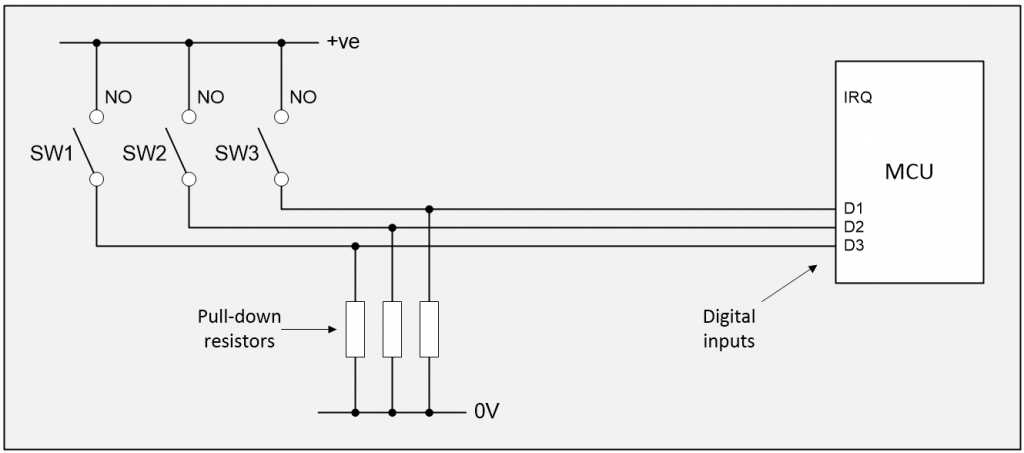
Multi-switch polling scenario (Image source: Max Maxfield)
In this context, the term “polling” refers to the MCU periodically sampling the state of the three digital inputs connected to the switches. We will consider this in more detail later. For the moment, let’s simply assume we have a main program loop that executes once every millisecond (ms). The first thing we might do at the start of every loop iteration is to poll (read) the state of each of the switches to see what’s going on.
The program would, of course, have to handle any switch bounce using one of the software techniques we are going to discuss. The main issue here is that the switches are only going to change state every now and then — once an epoch as far as the MCU is concerned — but we are checking them over and over and over again. Remember that, although we are showing only three switches here, in a real system there could be many, many more. None of this may be an issue, of course, unless we are working with an extremely resource constrained MCU in which we wish to jealously hoard every clock cycle.
Multi-Switch Interrupt Scenario (Raw)
As an alternative to the above, we could OR the signals from the switches and use the output from the OR gate to drive an interrupt request (IRQ) input on the MCU as illustrated below. (Note that when I was a bright-eyed, bushy-tailed young engineer, MCUs typically had only one or two dedicated interrupt inputs. By comparison, many modern MCUs allow the programmer to specify which pins they wish to act as interrupts, each with its own ISR.)
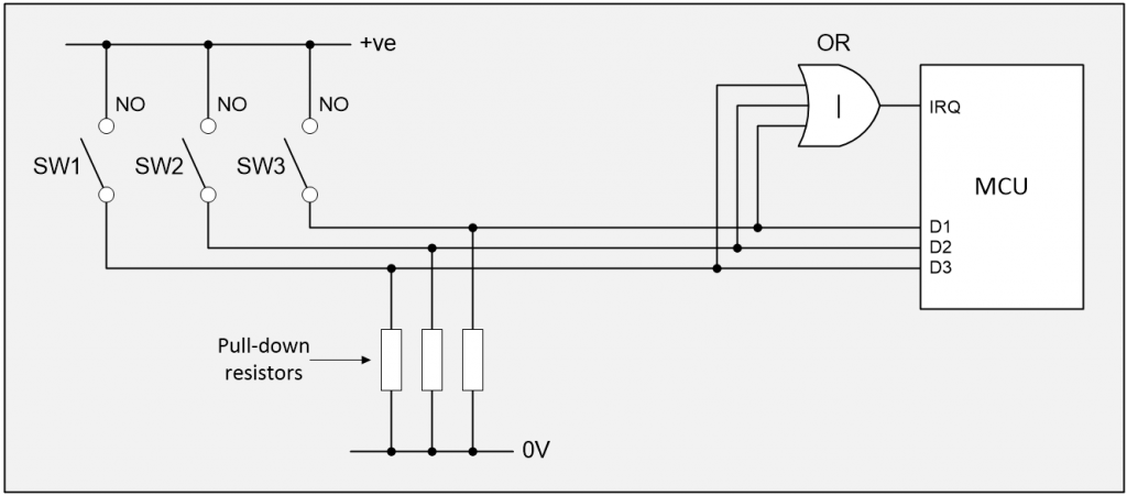
Multi-switch interrupt-driven scenario (Image source: Max Maxfield)
The idea here is that, assuming all of the toggle switches start off in their open (inactive) states, whenever one of the switches is closed, thereby connecting it to a logic 1, the output of the OR gate transitions from 0 to 1, generating an interrupt request. (The reason I used the “Raw” appellation as part of this topic title is that we are feeding raw (unprocessed, bouncing) signals into the OR gate.)
At this point, it’s up to the ISR to perform its magic, which could involve reading the states of the three digital inputs to see which one was activated. Alternatively, remembering that we want the ISR to be as small and fast as possible, it might simply set a flag to attract the attention of the main program and then return control to the main program.
Of course, we still have to worry about the fact that the switch might be bouncing like a yo-yo. There’s also the consideration that, unlike a radio pushbutton assembly whereby only one button may be active at a time, our toggle switches are not mutually exclusive. Thus, it’s possible for a second switch to be activated while the first switch is still active, but — since one of the OR gate’s inputs is already connected to logic 1 — this fact will never propagate through the gate to trigger a new interrupt request.
Bummer.
But turn that frown upside down into a smile, because all is not lost. In my previous column, we talked about the 3-channel LS118 debounce chip from LogiSwitch (6- and 9-channel versions are also available). Why is this of interest here? Read on…
Multi-Switch Interrupt Scenario (LogiSwitch)
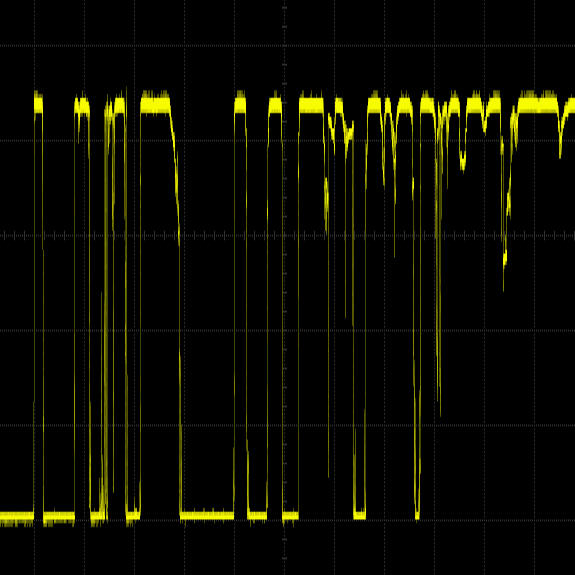
The first thing we noted about the LS118 is that its outputs are in the opposite phase to its inputs; that is, a logic 0 on a switch input will result in a logic 1 on the corresponding output. But the really cool thing about these devices is their unique 1-wire handshaking protocol. When the microcontroller (MCU) “sees” one of the NL/HS output signals from the LS118 go high, it can change its input pin into an output, pull the signal low for 50 microseconds (µs), and then return the pin to being an input.
The outputs from the LS118 are open collector with internal pull-ups. When the LS118 sees that the MCU is pulling one of its outputs low, it starts to drive that output low itself. The result is as illustrated below:
LogiSwitch LS118 chip reacting to switch bounce and using its handshake capability (Image source: Max Maxfield)
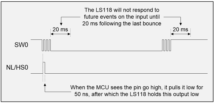
Bearing this in mind, let’s return to our system with three switches. If we wish to implement an interrupt-driven scenario using the LS118, we could do so as illustrated below:
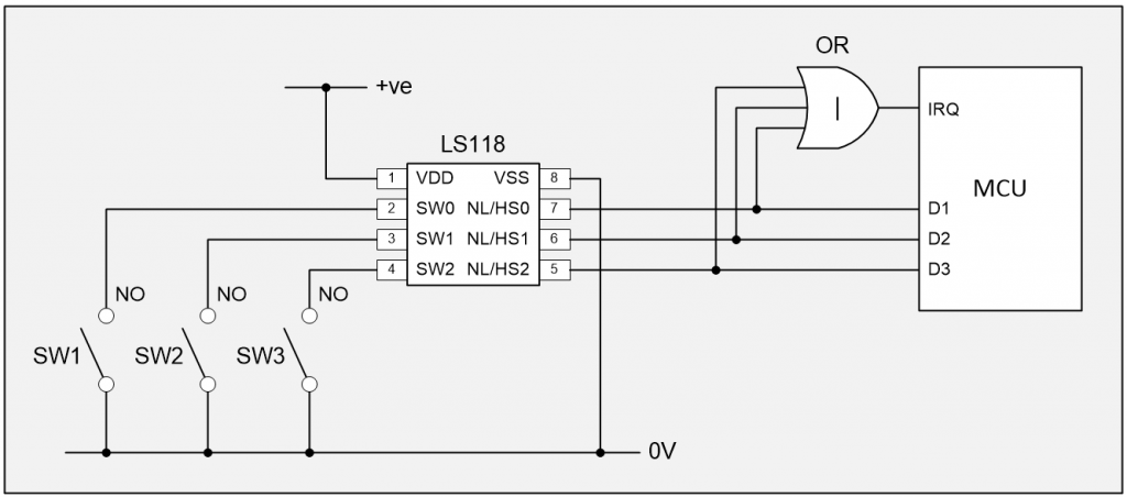
The LogiSwitch LS118 in a 3-switch circuit (Image source: Max Maxfield)
Once again, let’s assume that we start off with all of our switches in their open (inactive) states. When one of the switches is closed, thereby connecting that LS118 input to a logic 0, the corresponding output from the LS118 immediately (within a few nanoseconds) transitions to a logic 1.
This causes the output from the OR gate to transition from 0 to 1, thereby generating an interrupt request. Now, either the ISR or the main program can read the state of the three digital inputs to see which switch has been pressed, use the handshake protocol to clear that output from the LS118 back to a logic 0, and return to what it was doing. If another switch is subsequently activated, it will generate its own interrupt request (even if the first switch is still active, its output from the LS118 has been cleared to a logic 0).
Quite apart from anything else, since all of the switch debouncing is performed by the LS118, this means any interrupt-based handling of the switches is dramatically simplified as compared to dealing with everything in software.
Next Time
I’m really, really sorry. I’m not deliberately leading you on. It’s just that I always discover so much to talk about (much like my dear old mother, the real trick is getting me to stop talking). I absolutely promise — on my word as a Frenchman — that my next switch bounce column will be the final one in this series. In that column, we will cover hardware switch debouncing inside FPGAs and a variety of software techniques for switch debouncing in MCUs. Until that frabjous day, as always, I welcome your comments, questions, and suggestions.


Hello Max
I am following this series from the beginning. This was very informative ride 🙂 You don’t have to feel sorry, you are showing as many techniques about very popular problem.
I am interested in next column. FPGA has so many ways to handle the debounce.
thank you very much for series. I have not seen this topic discussed in this depth.
Thanks so much Pavle — I keep on worrying that people will think I’m dragging things on too long — but I know that when I started out, it seemed that people would explain things assuming that I already knew a lot of stuff, I didn’t actually have a clue — that’s why I like to explain things step by step the way I wish they had been explained to me “back in the day” 🙂
Quote from Jack ” So, if you have a bounce that lasts nanoseconds, will that mess up an internal flip-flop? Some people tell me it’s no big deal, as one of the bounces will get latched eventually. I feel this is poor engineering. It seems rash to tie something that might last less than a couple of clock cycles to an unknown input.”
So now, how many articles will it take to explain the meta-stability that messed up that internal flop?
Once upon a time there was a system that would “hang” every few weeks with no failed hardware.
Then there was another similar system had the same symptoms, but this time it was a mission critical system.
Wait just a minute , there was that “unity gain” problem that created havoc in a another system.
That was due to the synchronizing flop breaking into oscillation and eventually ending up reset instead of set. Does the word “Metastability” come to mind? But there was no switch therefore no switch bounce.
All it took was to add some hysteresis to the latch.
Ah — metastability — of course this really becomes important when interfacing external asynchronous inputs to FPGAs — in fact I was wondering about doing a column on this once I’ve finished waffling on about switch bounce (which, as I promised, will be my next column).
What say you — should I do a column (or two) on metastability?
I would be interested.
Clock domain crossing and arbiters are two obvious culprits.
And the third is as Jack wrote that people say “eventually it will get latched”. Phooey, that is not the whole situation. There will be glitches/splinter pulses and indeterminate switching levels that can create havoc.
People have been lead to believe stupid things “like everything happens at once” when the reality is that the most critical thing is sequences and interface handshaking protocols.
You know it is like everything was going great until it wasn’t because …
Max
This is a great series that keeps on giving. I wish I had had the courage to tackle the subject in the days that I used to write. However I feel there is a practical consideration that doesn’t really have any thing to do with switch bounce.
In your examples you have used switches that connect directly to Vcc. Over the years, several of my projects have run the supply off the board to external devices, often switches. A minor wiring error, loose wire or wire strand can pull the supply to ground (even with the switch open) since the chassis is normally tied to earth-ground. Unless there is some protection like a current limiting power supply or PTC resistors, you can end up with a soft error on the uC or worse ,a hard error including, but not limited to, tracks burned off the PCB if the current is high enough.
Of course it is possible to connect the one side of the switch to ground and use a pull-up resistor, but I don’t know if the LS118 handles this configuration. This is just one of many considerations when designing a robust circuit.
Hi Aubrey (a.k.a. antedeluvian) — you make good points as always — maybe this should become part of the curriculum for our “Finishing School for Electrical & Electronic Engineers” (https://www.clivemaxfield.com/finishing-school-for-electrical-electronic-engineers/)
I never take anything off a PCB that can source significant current unless that’s the purpose. For that reason, my switch inputs are always pull-up / switch-to-ground. That configuration also makes ESD protection more straightforward.
Dear Clive,
Any words of wisdom or experience on switch debounce in this scenario:
http://www.pcbheaven.com/wikipages/Charlieplexing/
Please scroll down to the heading “Charlieplexing also to interface buttons”
We charlieplexed 12 tactile push button NO key switches to 4 port pins of a PIC16F72. It worked but also kinda didn’t. Sadly that project got cancelled and the prototype was scrapped.
Regards,
Sid {A hardware guy who needs a lotta practice in embedded C};
Hi Sid — I only recently ran across Charlieplexing — it’s VERY clever. Re the switch bounce part, I’m up to my armpits in alligators at the minute, but I’ll ask Mike from LogiSwitch what he thinks (he LOVES switch debounce stuff 🙂