


I just turned 65 years old this past weekend. I find this fact hard to believe. Where did the time go? I don’t remember the 1980s at all (I must have had a bad beer). One of the cool things about growing older (there aren’t many, so you have to make the most out of what you can get) is that you’ve had the chance to perceive, peruse, and ponder a few things along the way.
For example, I got to see the very first episode of Doctor Who, which broadcast on Saturday 23 November 1963. I was 6 years old, I watched it from behind the sofa in our family room, and I can remember it to this day. I also got to see the first men land on the moon in 1969 with my dad when I was 12 years old. He gave me a small tot of whiskey and told me this was one of the most amazing things we would ever see in our lifetimes (this was long before I purchased my off-road unicycle, of course).
Over the years, I’ve also seen small startup companies come and go or grow. Take Lattice Semiconductor, for example, which was founded in 1983, went public in 1989, and has flourished to be the world’s largest volume supplier of FPGAs. Lattice is now a Tier 1 vendor with 39 years of innovation under its belt. The folks at Lattice tell me they will be celebrating their 40th birthday next year (I only wish I could say the same — LOL) so I’d better start planning which Hawaiian shirt I’m going to don for the festivities.
One reason for Lattice’s success is that they’ve created a cornucopia of FPGA families that are focused on addressing specific tasks, like their CrossLink families, which are targeted at video bridging and processing, and their Mach families, which address platform management and security. They also have their Certus families, which target a broad range of general-purpose applications, and their iCE40 families that address ultra-low-power applications.
Another reason for the company’s ascendancy is that, in 2019, the folks at Lattice introduced their Nexus Platform, which is based on a fully depleted silicon-on-insulator (FD-SOI) process. As I discussed in my Handling Radiation in SRAM-Based FPGAs (Part 1) and (Part 2) columns, by varying the biasing of the FD-SOI substrate, users can decide whether they wish to run for high performance (HP) or low power (LP). Even better, the system can switch back and forth in real-time under program control.
However, the really interesting thing about this process is that it is inherently radiation resilient. Quite apart from anything else, this process is immune to single event latch-up (SEL) conditions, which means there is no down-time in mission-critical situations that would normally demand a power cycle to exit the latch-up state. Lattice’s FD-SOI process also protects against single event upsets (SEUs), multiple bit upsets (MBUs), and multiple cell upsets (MCUs).
The reason I mention this here is that Lattice has just announced the most recent addition to its Nexus lineup – the MachXO5-NX.
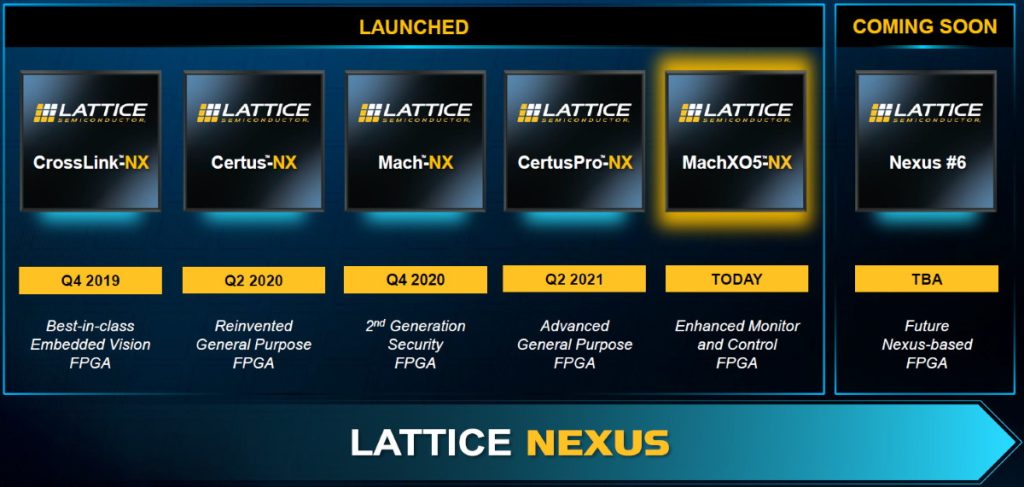
Say hello to the MachXO5-NX (Image source: Lattice)
These little scamps enable the latest generation of secure control through increased logic and memory resources, robust 3.3 V I/O support, and a differentiated security feature set. Designed to enhance system monitoring and control in the Server, Communications, Industrial, and Automotive markets, MachXO5-NX FPGAs offer class-leading power efficiency and reliability. A brief summary of these little rascals is as follows:
Increased logic and memory resources
- MachXO5-NX FPGAs combine a 25k logic cell capacity FPGA fabric with 1.9 Mb of embedded memory, reducing the design footprint by minimizing the need for external memory. The devices also offer up to 9.2 Mb of dedicated user flash memory to store mission-critical data and parameters.
- Integrated flash memory enables a single chip solution with instant-on operation and reliable in-field updates supporting multiple configuration images.
- MachXO5-NX FPGAs offer greater compute and control capabilities with added DSP and ADC blocks.
Robust programmable I/O
- MachXO5-NX FPGAs address challenges of modern CPUs and SoCs lacking robust 3.3 V I/O signaling support required to communicate with many other devices in system. The devices feature up to 300 general purpose I/O (80 percent supporting 3.3 V signaling) that support early I/O configuration and provide added features such as 1.25 Gbps SGMII, default pull-down, hot socketing, and programmable slew rate for simplified board design.
Class-leading Security
- On-chip multi-boot with bitstream encryption (AES256) and authentication (ECC256).
- Run-time security capabilities not currently available in competitive FPGAs of a similar class.
Leadership power efficiency and reliability
- Built on the Lattice Nexus platform, the devices deliver up to 70 percent lower power than competing FPGAs of a similar class offering simplified thermal management and reduced total system operating cost.
- Leveraging the FD-SOI manufacturing process, the devices provide up to 100 times lower soft error rate with improved system reliability than competing FPGAs of a similar class.
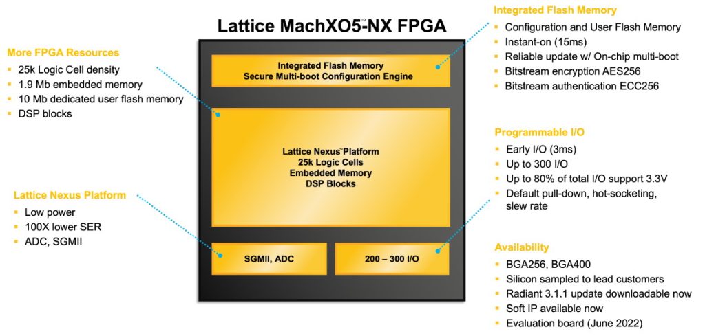
High-level block diagram of the MachXO5-NX (Image source: Lattice)
Take a look at the block diagram above. Is there anything that catches your eye? One thing that made me pause for thought is where we see “Secure Multi-Boot Configuration Engine.” In previous generations, this has been called “Dual Boot,” the idea being that you can have a golden image running in the device while you load a new configuration into the Flash memory. If the new configuration cannot be verified for any reason, then the device will continue to use its known-good golden image.
The reason “dual-boot” has morphed into “multi-boot” is that the MachXO5-NX now boasts enough Flash configuration memory to support three images, which opens the door to a wealth of configuration possibilities and potentialities.
“A picture is worth a thousand words” as the old adage goes (this is especially true with regard to yours truly and his aforementioned off-road unicycle), so feast your orbs on the following:
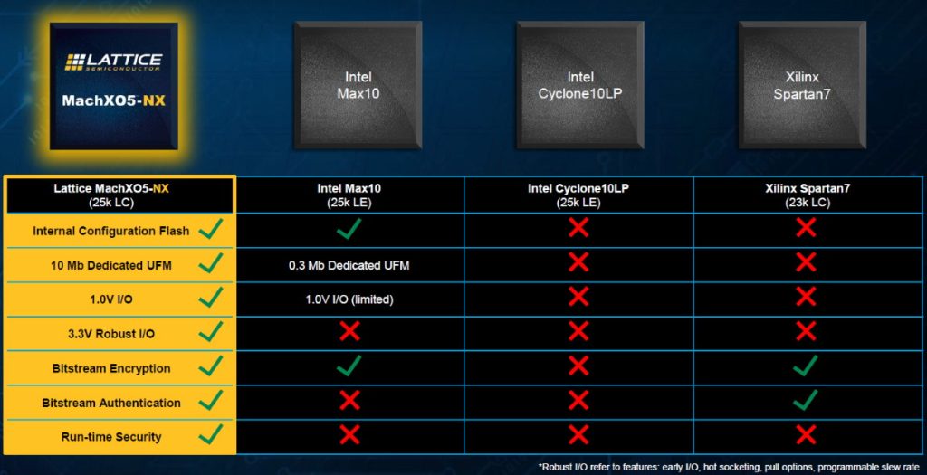
Simplify system design with MachXO5-NX FPGAs (Image source: Lattice)
To be honest, I think this says it all, and I have nothing to add, so this is where we spin around three times and turn our attention to Lattice’s other nugget of noteworthy news, which is the introduction of the new ORAN Solution Stack.
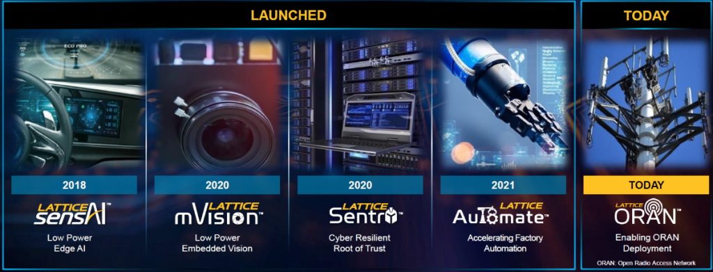
I’m sure you are familiar with Lattice’s solution stack concept. These bodacious beauties provide turnkey application-specific solutions that combine reference platforms and designs, demos, IP building blocks, FPGA design tools, and custom design services to accelerate customer application development and time-to-market.
The Lattice solution stacks portfolio includes solutions for market applications including AI with Lattice sensAI, embedded vision with Lattice mVision, platform firmware resiliency root of trust (RoT) with Lattice Sentry, factory automation with Lattice Automate, and now 5G ORAN deployment with the new Lattice ORAN solution stack.
Meet Lattice ORAN, the new member of the solution stack family
(Image source: Lattice)
According to Kenneth Research, the global Open Radio Access Network (O-RAN) market is expected to become a $22B market by 2028 with an 85 percent CAGR between 2020 and 2028, driven by the rapid adoption of 5G technology. To keep pace with this growth, the communications industry is increasingly embracing the disaggregation and openness of ORAN as drivers of increased flexibility, innovation, and cost reduction. This open environment requires safe and secure communication, tight synchronization across multiple components, and efficiency with low-power hardware acceleration.
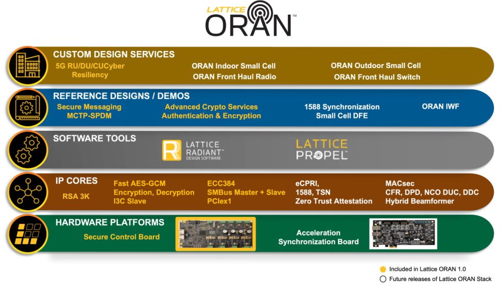
The multi-layered offering that is Lattice ORAN (Image source: Lattice)
The Lattice ORAN solution stack is a complete turnkey solution for 5G customers looking to secure data, accelerate network function, and achieve tight synchronization. A brief summary of what the Lattice ORAN solution stack offers is as follows:
Robust zero trust security
- Authentication with real-time encryption and decryption functions.
- Ready-to-use software.
- RISC-V software included to configure security functions.
- Lattice Propel and Lattice Radiant to fully customize and implement security in ORAN applications with its intuitive design interface.
Tight synchronization for flexible fronthaul in future release
- IEEE 1588 protocol targeted to maintain the strict timing and synchronization requirements between the Radio Unit (RU) and Distribution Unit (DU) to support New Radio (NR) protocols, including enhanced Common Public Radio Interface (eCPRI).
Acceleration with low power and high reliability
- Up to 70 percent lower power and up to 100 times more resistant to soft errors in the smallest form factor than competing FPGAs of a similar class.
Well, I don’t know about you, but I think that’s about all the excitement I can handle for one day (when you get to my age, being presented with too many exciting things in one sitting can be a tad taxing). What say you? Do you have any thoughts you’d care to share about anything you’ve read here – like how wonderful Lattice is, how wonderful I am, or how getting old isn’t as much fun as we’d hoped it would be? Suffice it to say that the comment area below this column is quivering in the anticipation of receiving your captivating communiqués.


