

As we discussed in Part 1 of this two-part mega-mini-series, radiation in its various forms has long been the bane of designers of electronic systems, and the effects of radiation become more insidious and pervasive as integrated circuit fabrication processes employ smaller and smaller structures.
We also introduced the concepts of electromagnetic radiation (EM radiation or EMR), whose force carrier is a massless particle called a photon, along with radiation in the form of particles with mass — predominantly electrons, protons, neutrons, and atomic nuclei stripped of their electron shells. When any of these particles can impart enough energy to strip away one or more electrons when it hits an atom or a molecule — including the atoms forming the crystal lattice in a semiconductor — leaving a positive ion in its wake, then that particle is referred to as “ionizing radiation.”
One topic we didn’t mention, but that is relevant to our discussions, is that of “cosmic rays.” In fact, the “ray” portion of this moniker is a misnomer based on a historical misstep. When they were first detected, cosmic rays were incorrectly believed to be mostly EMR in the form of X-rays and gamma rays. It was later discovered that cosmic rays are very high-energy particles that predominantly originate outside our solar system and that result from cosmic events such as supernovae.
Of the primary cosmic rays, which originate outside of Earth’s atmosphere, about 99% are the nuclei of well-known atoms, while about 1% are solitary electrons. Of the nuclei, about 90% are simple protons (i.e., hydrogen nuclei), 9% are alpha particles (i.e., helium nuclei), and 1% are the nuclei of heavier elements. (A very small fraction comprises stable particles of antimatter, such as positrons or antiprotons.) When a primary cosmic ray hits the Earth’s atmosphere, it may produce showers of secondary particles that penetrate the atmosphere and sometimes even reach the surface of the planet.
The most energetic ultra-high-energy cosmic rays (UHECRs) that have been detected thus far approach ~40 million times the energy of particles accelerated by the Large Hadron Collider (LHC). The highest-energy cosmic rays observed up to now have energies comparable to the kinetic energy of a baseball travelling at 90-kilometers-per-hour (56 mph). I don’t know about you, but the thought of this makes my eyes water. Can you imagine the effect of all that energy being concentrated in a tiny area in an integrated circuit?
Just What Is an SRAM-Based FPGA?
The focus of this column is mitigating radiation effects in SRAM-based FPGAs. Unfortunately, in the past, I’ve found some people are confused by the term “SRAM-based” on the basis that the programmable fabric of any modern FPGA contains blocks of SRAM, along with registers and combinatorial logic in the form of look-up tables (LUTs), multiplexers, and other “stuff.”
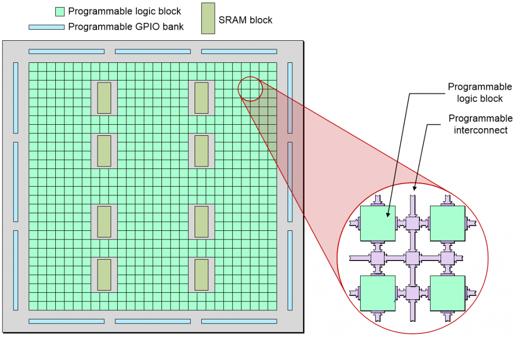
Highly simplified depiction of an FPGA’s programmable fabric
(Source: Max Maxfield)
I always think of an FPGA as being comprised of myriad little “islands” of programmable logic in a “sea” of programmable interconnect. The thing about an FPGA — its defining feature, you might say — is that it can be programmed (configured) to perform almost any combination of logical functions that its designers desire. This is achieved by means of configuration cells, which — amongst other things — are used to define the functions of the logic blocks and the ways in which these blocks are connected to each other and to the outside world.
The configuration cells may be realized using a variety of implementation technologies, such as antifuse cells, flash cells, and SRAM cells. Thus, when we refer to an FPGA as being “antifuse-based” or “flash-based” or “SRAM-based,” we are talking about the technology used to implement its configuration cells.
Antifuse-based configuration cells are all but immune to the effects of radiation, but they are one-time programmable (OTP), which means that once you’ve programmed the device, there’s no turning back. On the other hand, these devices are non-volatile (they remember their configuration when power is removed from the system), which means FPGAs implemented using this technology are “instant on.”
Flash-based configuration cells are also non-volatile, so FPGAs implemented using this technology are also “instant on.” Apart from anything else, this makes them ideal for power management control applications in which they are the first device to be powered on and the last device to be powered off. Unlike antifuse-based FPGAs, flash-based devices can be reprogrammed. To be honest, I was under the impression that flash-based configuration cells are relatively immune to the effects of radiation, but earlier today as I pen these words, I received a message from Peter Smith, CEng, who said: “I spent years analysing the probability of SEUs in avionics. At altitudes below 100,000 feet, the biggest threat is free neutrons. (Tidbit: Flash cells are quite susceptible to X-rays)”
Finally, we have SRAM-based configuration cells. These are volatile (they forget their configuration when power is removed from the system), which means FPGAs implemented using this technology require their configuration to be loaded when power is first applied to the system. A big advantage of FPGAs with SRAM-based configuration cells is that they can be implemented at the latest and greatest CMOS technology nodes. By comparison, antifuse and flash-based devices require additional processing steps, so they typically lag their SRAM-based counterparts by one or two technology nodes.
Returning to the focus of this column, there are two aspects to SRAM-based FPGAs that we need to consider: (a) the registers, the memory cells in the SRAM blocks, and the combinational logic as seen by the designer and/or user, and (b) the SRAM-based configuration cells used to program the device. Let’s start with the logic as seen by the designer, and then move on to consider the configuration cells.
Mitigating SEUs at the Register Level
In Part 1 we introduced the concept of single event effects (SEEs), which may also be referred to as single event phenomena (SEPs), that can be triggered by an individual radiation event. A single event upset (SEU) is a SEE that occurs when a radiation event “flips” a register bit or memory cell (changes its contents from a 0 to a 1, or vice versa).
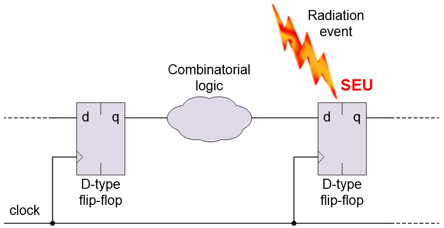
A single event upset (SEU) causing a register bit to flip (Source: Max Maxfield)
In the case of a register, one way to mitigate an SEU is to implement triple modular redundancy (TMR) at the register level. This involves creating three copies of the register as illustrated below.
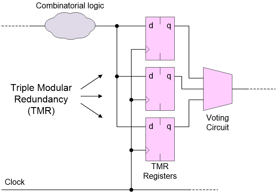
Mitigating SEUs by implementing triple modular redundancy (TMR) at the register level (Source: Max Maxfield)
A voting circuit is employed to accept a majority (two out of three) vote from the three registers. In this case, the SEU will be restricted to the affected register, and it will be automatically cleared out of the system on the next clock cycle.
Mitigating SETs at the Register Level
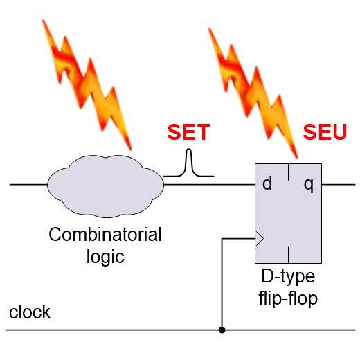
Another form of SEE is a single event transient (SET), which is a radiation event that strikes a chunk of combinatorial logic resulting in a pulse, glitch, or spike.
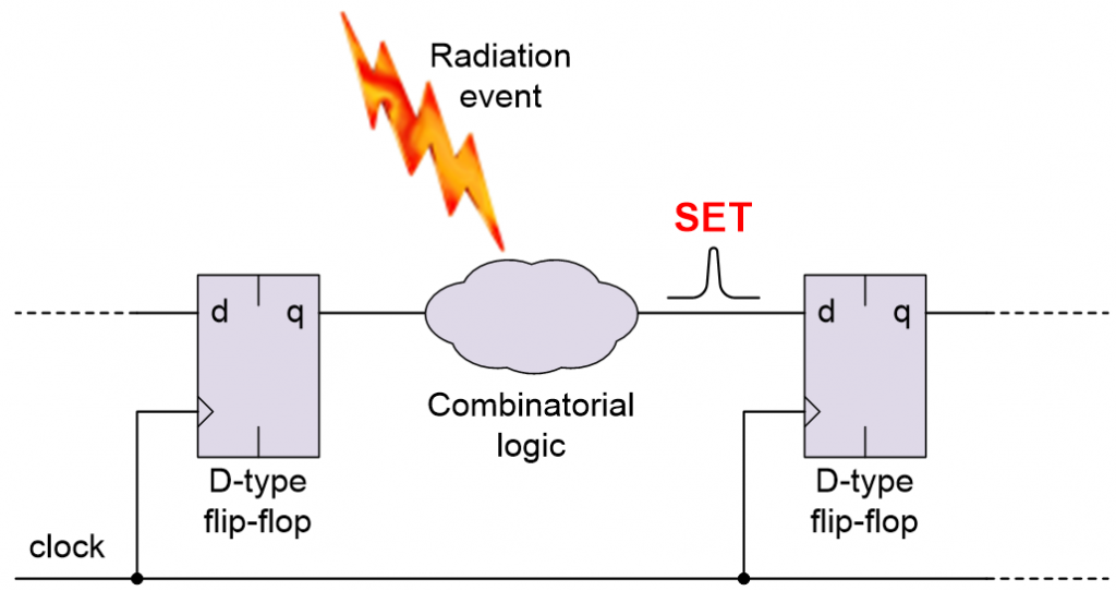
A single event transient (SET) in the combinatorial logic (Source: Max Maxfield)
If the SET has cleared before the next clock arrives (and assuming it doesn’t violate the downstream register’s setup or hold times), then there isn’t a problem. However, if the SET is clocked into the downstream register and/or causes that register to enter a metastable condition, then the SET will be converted into an SEU.
One way to mitigate against a SET is to delay the output from the combinatorial logic so as to “stagger” the way in which it reaches the inputs to the TMR registers.
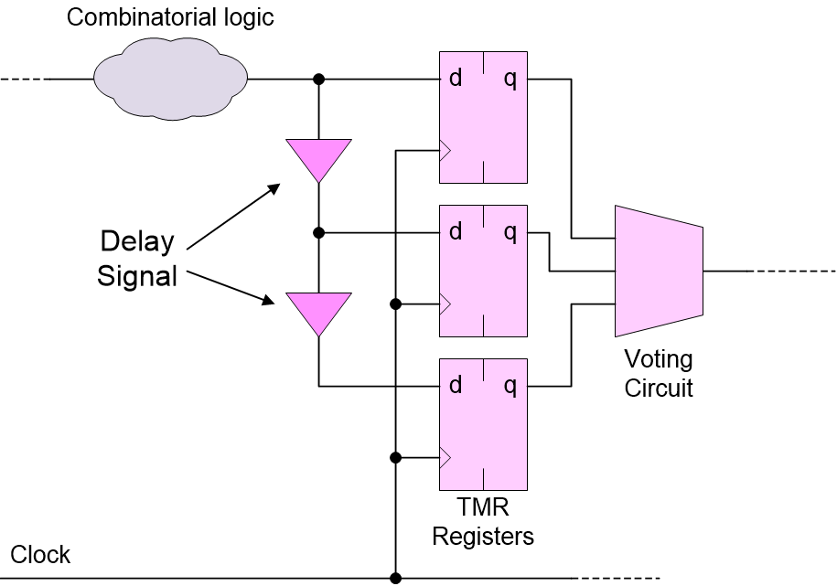
Mitigating SETs by adding delays (Source: Max Maxfield)
Another area of concern is SETs and SEUs causing transitions into invalid states – or invalid transitions between good states – in finite state machines (FSMs), but that’s a topic for another day.
Mitigating SETs and SEUs at the Design, Chip, Board, and System Levels
In the not-so-distant past, radiation was primarily considered to be a problem for the aerospace industry, especially in the case of systems like deep space probes travelling to hostile environments like the environs of mighty Jupiter and its moons.
The point is that the creators of such systems used to have deep pockets, and they were prepared to pay extravagant sums of money for special-purpose FPGAs that boasted features like SET delay elements and TMR at the register level. I believe that these little rascals could cost as much as US$140K for a relatively low performance, low capacity device, which would certainly give me pause for thought.
Another issue was that these devices were based on antifuse technology, which is one-time programmable (OTP). This minimized radiation concerns insofar as the configuration cells were concerned, but it also meant that the designers lost access to one of the key advantages offered by reprogrammable FPGAs. Once something like the Curiosity Rover has landed on Mars, or the New Horizons space probe has passed Pluto and is winging its way to visit other objects in the Kuiper belt, things can get a tad awkward if something goes wrong or you discover a better way to do things but your FPGAs cannot be reprogrammed.
These days, even the military and aerospace industries are starting to count pennies, which means they are increasingly amenable to using commercial off-the-shelf (COTS) devices. One solution to the radiation problem is to use regular off-the-shelf FPGAs and to perform TMR at the design level by replicating the design three times in the same device and then performing the voting function on the outputs of the design.
Happily, some tool suites allow the developer to simply say, “I wish to apply TMR to this portion of the design,” and the tools make it so, which removes a lot of the pain and the potential for messing things up. One thing to consider here is that it may not be necessary to actually TMR all aspects of the design. Suppose we have a satellite taking high-resolution images of the Earth, for example. Each image may be first stored and pre-processed in SRAM in the FPGA. Now suppose a radiation event causes a single bit in the image to be flipped. Do we really care? The resulting artifact may well be filtered out by any image processing algorithms, and a new image will be taken almost immediately. By comparison, in the case of a block of SRAM containing any critical flight control variables and routines, we would absolutely want to TMR this block and use any other techniques at our disposal to maintain the integrity of its data.
Speaking of which, we would also want any of our FPGAs deployed in hostile environments to use error correcting code (ECC) memory, which refers to memory implemented in such a way that it can be used to detect and correct any internal data corruption, such as that caused by a radiation event. In Part 1, we noted that SEUs are referred to as “soft errors” because they can be corrected (if you know what you are doing). Well, this leads to the concepts of soft error detection (SED) and soft error correction (SEC).
Furthermore, the term “memory scrubbing” refers to periodically reading from each memory location, correcting bit errors (if any) with an error-correcting code, and then writing the corrected data back to the same location. In addition to mission-critical and safety-critical systems, memory scrubbing is also used in systems that are subject to high radiation environments.
As opposed to performing TMR by replicating the design in a single FPGA, we might decide to perform TMR on the FPGA itself; that is, to have three copies of the FPGA on the board and to perform the voting function on the outputs of the chips. Alternatively, we might decide to perform TMR at the board level or at the system level.
For some applications, TMR might be considered to provide only a starting point. There’s also quadruple modular redundancy (QMR), which uses four units instead of three to increase the reliability, and designers may opt to use more units as required.
In truly extreme cases, the creators of the most mission-critical and safety-critical systems may decide to have multiple versions of a design implemented by disparate teams using dissimilar tool chains and incongruent implementation technologies. The voting function would then be performed on the outputs of these independent implementations. I’m not sure what the official name for this is, so let’s call it “hardware diversity” until someone tells us different. The sad thing is that, even if we were to go to these extremes, we wouldn’t necessarily eliminate all possible errors, since everyone would be working from the same core specification and many issues stem from specification ambiguity.
MCUs, MBUs, and SELs
Is it just me, or are there more TLAs (three-letter acronyms) than there used to be? I’m starting to understand why glazed looks come over the eyes of my family and friends if they imprudently ask me what I’m writing about and I foolishly try to tell them.
Before we proceed further, it’s probably worth noting that our earlier discussions may have been a little misleading. For example, I’m thinking of the part where we noted that “When any of these particles can impart enough energy to strip away one or more electrons when it hits an atom or a molecule…”
Unfortunately, some people understand this to mean that only a single atom or molecule is affected. The truth is a little more… let’s say “exciting.” Consider the image below.
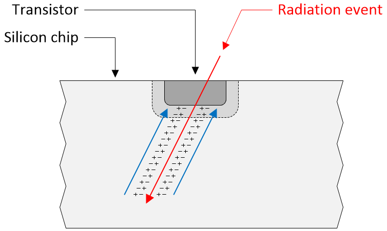
A radiation event leaves a trail of “excitement” (Source: Max Maxfield)
When a radiation event (red arrow) in the form of an energetic particle travels through the silicon, it leaves a trail of +/- charges in its wake. These charges subsequently collect at the incident node (blue arrows).
But wait, there’s more, because when we talk about a single event upset (SEU), we tend to think about it affecting a single register element or memory cell, but this is not necessarily the case. Sad to relate, ever shrinking fabrication processes are resulting in a trend toward memories experiencing multiple cell upsets (MCUs). What this means is that, since the structures in the silicon are now so close together, an SEU may actually upset multiple memory cells as illustrated below.
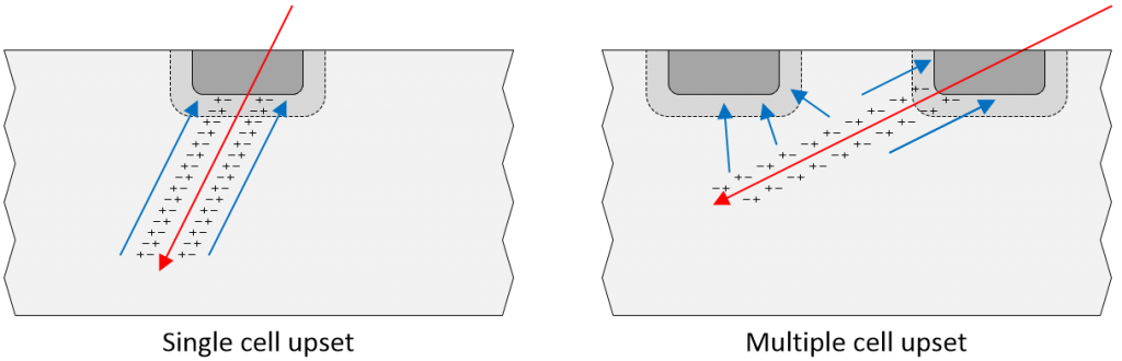
A radiation event may affect a single memory cell (left) or multiple memory cells (right) (Image source: Max Maxfield)
Furthermore, the term multiple bit upset (MBU) refers to a MCU that occurs within the same data word or frame, which may negatively impact the system’s ability to correct the error.
Last, but certainly not least, with regard to our discussions here, we also have to worry about a radiation event triggering a single event latch-up (SEL). This refers to the creation of a low-impedance path (effectively a short-circuit) between the power and ground rails in a CMOS circuit. If an SEL occurs, the device needs to be immediately power cycled (turned off and on again) in order to prevent serious damage. It probably goes without saying that having to power cycle a system may be problematic in many situations.
Mitigating Radiation Events in SRAM Configuration Cells
There are almost invariably many different ways to do things. In the case of SRAM-based configuration cells, for example, one technique is to constantly scan the configuration cells and generate a cyclic redundancy check (CRC) value based on their contents. This CRC is then compared to a “Golden CRC” associated with the current configuration. If a mismatch is detected, the system can be paused while the FPGA’s configuration is reloaded.
A sophisticated version of this can be employed when TMR is applied to the design inside a single FPGA. In this case, the configuration associated with the affected copy of the design can be reloaded while the other two copies continue to function.
Back in 2011, the folks at Xilinx introduced their 65 nm “Space Grade” Virtex-5QV FPGA. As opposed to the 6-transistor (6T) configuration cells used in regular SRAM-based FPGAs, the Virtex-5QV boasts 12T configuration cells. In this case, each cell is formed from a dual interlocking latch that can be “flipped” only by the direct ionization of dual complementary nodes. This is not a matter of simply employing redundancy by creating a duplicated 6T cell. In the case of the 12T cell, every point in one half of the cell has a complementary point in the other half, and the same ionizing particle has to upset both complementary points for the cell’s value to become corrupted.
This really is a clever idea, but it does result in a huge overhead because FPGAs can contain millions of configuration cells. Also, having special devices targeted at narrow markets means that the price of those devices doesn’t land in the “cheap-and-cheerful” portion of the cost curve (“If you have to ask, you can’t afford it,” as the old saying goes).
While I think about it, there’s one more point that may be of interest to users of flash-based FPGAs who feel confident that flash configuration cells are relatively immune to the effects of radiation. In many cases, the flash configuration memory is implemented as a distinct block on the chip. This block is accompanied by “shadow” SRAM configuration cells that are distributed across the face of the chip. When power is first applied to these devices, the configuration is copied in a massively parallel fashion from the flash configuration memory into the SRAM configuration cells, at which point we’ve just returned to having to worry about radiation events flipping our bits (I hate it when that happens).
Eliminating SETs, SEUs, SELs, MCUs, and MBUs at the Chip Level
Having things like TMR at the register level and special 12T configuration cells is all well and good, but wouldn’t it be nice if we could prevent most radiation-induced effects from occurring in the first place?
Well, you can only imagine my surprise and delight to discover that those little scamps at Lattice Semiconductor have done this very thing. Using Samsung’s 28 nm fully depleted silicon on insulator (FD-SOI) process, the guys and gals at Lattice have introduced their Nexus Platform (at the time of this writing, Lattice is the only low-power FPGA vendor using the FD-SOI process).
By varying the biasing of the FD-SOI substrate, users can decide whether they wish to run for high performance (HP) or low power (LP). Even better, the system can switch back and forth in real-time under program control.
But the really interesting thing about this process in the context of this column is that it is inherently radiation resilient. Quite apart from anything else, this process is immune to SEL conditions, which means there is no down-time in mission-critical situations that would normally demand a power cycle to exit the latch-up state.
As we previously discussed, when a radiation event in the form of an energetic particle travels through a register element or a memory cell, it ionizes the semiconductor material (charge generation) and creates a brief current pulse (charge collection). This current pulse may be sufficient to disturb the stored value, resulting in an SEU.
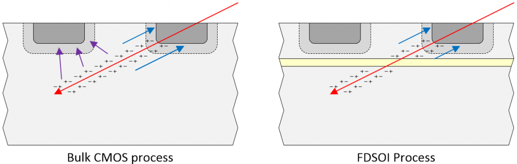
Let’s start by considering the representation of a bulk CMOS process as depicted below. The radiation event (red arrow) generates an ionized path through the silicon leaving a trail of +/- charges in its wake. These charges subsequently collect at the incident node (blue arrows).

SEUs: Comparison of the effects of a radiation event on a bulk CMOS process (left) and an FD-SOI process (right) (Image source: Max Maxfield)
By comparison, in the case of the FD-SOI process, the layer of buried oxide (yellow) isolates the node from the bulk of the generated charge. Any charge below the oxide layer is unable to collect at the sensitive node. Less charge means smaller transient current pulses, and smaller transient current pulses are less likely to upset register elements or memory cells.
Even better, the FD-SOI process protects against MCUs and MBUs. Once again, let’s start by considering the representation of a bulk CMOS process as depicted below. As before, the radiation event (red arrow) generates an ionized path through the silicon leaving a trail of +/- charges in its wake. In this case, in addition to collecting at the incident node (blue arrows), these charges may also collect at an adjacent node (purple arrows), possibly resulting in an MCU or MBU.
MCUs and MBUs: Comparison of the effects of a radiation event on a bulk CMOS process (left) and an FD-SOI process (right) (Image source: Max Maxfield)
By comparison, in the case of the FD-SOI process, the layer of buried oxide (yellow) dramatically shrinks the sensitive area of each cell, thereby making it much more difficult for a single particle track to affect multiple bits. In turn, this results in a substantial decrease in the generation of MCUs and MBUs.
Reducing the FIT Rate to Virtually Zero
Designers of mission-critical and safety-critical systems use the concept of the FIT (failures in time) rate. The FIT rate of a device is the number of failures that can be expected in one billion (109) device-hours of operation, (e.g., 1 device for a billion hours, 1000 devices for 1 million hours each, 1 million devices for 1000 hours each, or some other combination thereof).
In the case of a typical FPGA implemented in a bulk CMOS process at the 28nm technology node, the FIT rate is about 100. By comparison, in the case of a Lattice FPGA implemented using the Nexus Platform’s FDS-OI process at the 28nm technology node, the FIT rate is only 1. This means that, right from the get-go, the Nexus Platform provides an improvement in FIT rate of two orders of magnitude.
But this is just the start, because the chaps and chapesses at Lattice are on a mission to bring the FIT rate down to zero. The first FPGAs to be introduced based on the Nexus Platform is the CrossLink-NX embedded vision and processing family..
Earlier, we briefly mentioned the concepts of error-correcting code (ECC) memory, soft error detection (SED), soft error correction (SEC), and memory scrubbing.
Designers typically have to implement memory scrubbing functionality themselves, thereby consuming valuable programmable logic resources. By comparison, CrossLink-NX FPGAs include hardened intellectual property (IP) blocks that automatically perform ECC-based memory scrubbing as a background process.
In the case of their SRAM-based configuration memory, CrossLink-NX FPGAs have an in-built SED/SEC block to facilitate rapid detection and correction of errors on a frame-by-frame basis without the need for external circuitry. Although such errors are exceedingly rare for the reasons discussed above, they are theoretically possible. Happily, even if a radiation event were to somehow cause a configuration cell to flip state, this hard IP would flip it back again.
So Much to Learn, So Little Time…
The ways in which radiation can affect electronic circuits and systems is a huge topic. In reality, we’ve barely scraped the surface here (we didn’t even consider how radiation can affect analog and mixed-signal integrated circuits, for example).
Having said this, I think we took an appreciable bite (well, maybe a large-ish nibble) out of this subject. I know I get excited by technology in general, but I must admit to being particularly enthused by Samsung’s 28 nm FD-SOI process and Lattice’s Nexus platform. I think it’s awesome that we now have SRAM-based FPGAs that we can use in exciting projects like deep space probes while taking full advantage of their reconfigurable nature, unlike the technologies of yesteryear that left us longing for more.
What say you? I would be extremely interested to hear about your experiences with radiation affecting electronic systems, along with any radiation-related nuggets of knowledge and tidbits of trivia you would care to share in the comments below.


Awesome article! Very informative. Love the logic diagrams and graphics.
You’re making me blush!
(Don’t stop! 🙂
Thank you very much for your kind words — I really appreciate hearing from people who take the time to read my meandering musings 🙂
FIT is a generic unit of measure for describing very low failure rates, not a metric in and of itself. In the context of this article, you are describing the Soft Error Rate (SER) in FIT. As an alternative use: an automotive safety engineer would use FIT to describe a component’s random failure rate (bottom of the bathtub curve).
People that know what they’re looking at can usually distinguish what’s being referenced, but it’s a bad practice to only reference a metric only by its unit of measure. For example, consider describing pool water with “The PPM Rate is 15”. Without context, this makes no sense: what are you measuring? Chlorine, salt, debris??
Hi Schroz — you make a good point — I will try to explain things better next time 🙂