


It’s an idea rooted in the very identity of the products that the semiconductor industry puts out: the integrated circuit (or IC). For decades, our job has been to take lots of things that used to exist as separate components – transistors, resistors, capacitors, and such – and build them all in close proximity on a single monolithic piece of silicon.
From our initial efforts, we achieved simple logic chips and analog circuits. Gates and op amps.
But then we got better at putting things together, and we combined gates into purpose-built logic chips, like processors, and no-purpose-yet logic chips – programmable logic. We upped the analog ante to bring smaller components together as full-on filters and power ICs.
And then we found that, if we work hard, we could bring together things that hadn’t worked well together in the past, like microcontrollers (MCUs) with integrated flash, RF chips with both digital and analog/RF circuits. There was even talk of putting MEMS, analog, and digital circuits together as single-chip solutions. But this happened about the time we started rethinking our integration religion.
What were some of the issues that fueled this new apostasy?
- Really big chips, with more stuff on them, are harder to get to yield than smaller chips. A flaw in one place will kill an entire big chip. If, instead, there were 10 smaller chips in that same area (again with only the one flaw), then 9 out of the 10 would have yielded.
- Integration requires compromise. The flash that goes into an MCU doesn’t use the same specialized technology that’s used in high-density memory-only flash chips. As memory gets denser – with things like 3D NAND flash – it becomes even harder to put that on a standard logic chip.
- Digital circuits scale well with each new technology node; analog circuits, not so much. Once an analog circuit is working, the temptation is to leave it alone, foregoing potential shrinks. If the digital portion of a mixed-signal chip needs a new process node, then the analog part will need to be redone on that node. That’s a lot of work.
- Some chips need specialized materials, like wide-bandgap semiconductors. It certainly costs extra to put that on a small chip for use where it’s truly needed; adding such materials to a large, highly integrated chip adds that cost to the whole thing, raising the cost of the parts of the circuit that don’t benefit from these materials.
- Chips often need options. No category of IC shows this more than programmable logic, of which FPGAs are the overwhelming majority these days. If you’re building a big FPGA, some folks may need high-speed chip-to-chip interconnect, some may need this memory, some may need that memory, and others may need some analog circuits. How do you come up with an architecture that has what people need without adding the kitchen sink, most of which will stay idle on any given design? Even for fixed-function chips, there will still be options. Do you blow out your product offering to have all possible versions of your chip?
What’s Old is New
So, if integration is no longer the belle of the ball, then what’s the alternative? Actually, it’s been around for a long time – even if its original name isn’t used much these days. The multi-chip module (MCM) has a venerable history, but for a long time, it was viewed as a clunky solution of chips on a board with a metal can around the whole thing. It achieved limited success.
So what’s changed? Well, for one, we have sophisticated new ways to put chips together, what with wafer-level packaging options, interposers for 2.5D integration, and outright 3D chip stacking. These allow much finer-pitched connections than a standard PCB can handle. Connection technology – once pins on a DIP package, then leadless leads and arrays of balls – have evolved significantly. We now have bumps and micro-bumps that can make available far more signals with greater performance and lower power than was possible before. Clunky no more.
Efforts to leverage these new technologies have been in the headlines a few times over the years, with lots of research papers and lots of PowerPoint-ware. The term system-in-package, or SiP, has reflected early efforts. But things appear to be coalescing into something more universal and scalable. It’s the notion of the chiplet, and it’s explicitly about taking apart the chips that we have worked so hard to integrate over the years.
Despite the “chiplet” name, we can’t look at these simply as small chips. Chiplets couldn’t be used by themselves; they’re specifically intended to be lego-ed together to build complete functionality. It’s probably better to think of chiplets as design-IP-on-silicon. Instead of buying that RTL or GDSII IP to add to the chip you’re building, you build your chip and then connect it to a chiplet to get the same functionality.
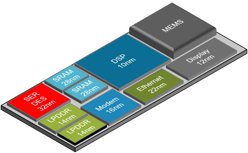
(Image courtesy Cadence)
Building a Chiplet Market
Which, of course, raises a critical topic for this to work: interoperability. The vision is that, just as there is a thriving market in design IP today, there would be a thriving market in chiplets. Multiple vendors would compete on performance or power or price or features or reliability – the same way chip vendors and IP vendors compete today.
But that works only if you can create your chip with an interface that allows it to hook up to any chiplet of choice. If there are no interconnect standards, then you have to wait to design your interface until you’ve selected your chiplet. After that point, you’re locked in – you can’t opt for a different vendor in the future.
These interconnect schemes can be far different from large-scale approaches like PCIe. By relying on micro-bumps attached to interposers (or alternatives like Intel’s EMIB approach) and much shorter runs, you can pack far more signals together and run them at much higher speeds than would be possible if you were using standard packaging interconnect. Standards for both serial and parallel interconnect are materializing (a topic we may take on in a future article).
While the following figure is a drawing rather than a photograph, it illustrates the scale of shrink that is available. And note that we’re not only breaking off chunks of chips to be used separately; we’re also now able to include things like memories that have started as separate chips, making them more tightly interconnected without being truly (i.e., monolithically) integrated.
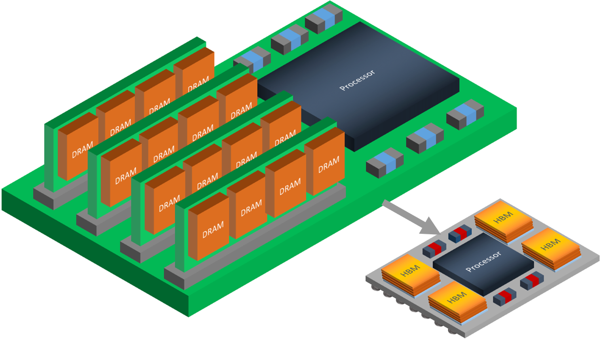
(Image courtesy Cadence)
How to Design Such a System??
But this disintegration of chips mandates better integration of another sort: design tools. With full silicon integration, you rely on chip-design tools to do everything, and then you hand that off to a package. The packaging folks have worked out how the package performs in their own set of tools. Then the packages are attached to a board, with yet another set of tools to manage the board-level issues. You have at least three different domains – the first of which handles all of the chip behaviors and the rest of which deal only with signal interconnect.
With a chiplet strategy, the only true picture of full functionality comes from a combined view of chips and interconnected chiplets, including the package-level characteristics (balls and bumps) and the substrate characteristics (no longer a PCB, but some kind of interposer or even another chip). How the heck do you manage that??
This was the topic of a conversation I had with Cadence at the recent DAC conference. They talked about the full range of tools necessary to bring everything together:
- In their world, their PCB tool Orbit serves as the “top level.” Orbit 10 is no longer specifically only about PCBs, but it manages chips and chiplets collocated on some surface
- Digital design tools cover the detailed design of logic circuits, as usual.
- Analog design tools like Virtuoso cover the detailed design of analog and custom circuits, as usual.
- Design tools must be able to handle multiple pieces of silicon – not as usual.
- Full analysis means treating a signal between chips and chiplets as heterogeneous connections that start at the output of a transistor on one piece of silicon, move to and then go through an interconnect bump, move through an interposer, re-enter another piece of silicon through another bump, and then travel on-chip until the target transistor is reached. Full 3D solvers (like Cadence’s recently announced Clarity) may be necessary to cover all design and verification aspects.
Where This Stands Today
Right now, we’re ahead of a full market for this technology. Efforts underway tend to be fully in-house, with a single company creating its own chiplets and bringing them together. Cadence sees it being 3-5 years before we get a real market.
There’s one other notion that bears reviewing in light of this development. There has been a lot of effort in making all kinds of processes compatible with CMOS. Heck, even MEMS companies have worked on this. An obvious benefit of doing so is that you can then integrate MEMS (or RF or whatever) onto a CMOS chip. With the advent of chiplets, is that going to stop?
Perhaps to some extent, but not entirely, in my opinion. Where materials and process differences add real value, then one can go without the compromises required for full CMOS compatibility. But there is one good reason to be CMOS-compatible, if you can, even if not for integration: because CMOS is so mainstream. If you make a chip on a boutique process, then customers are going to question closely whether or not the process is manufacturable with good yields and high volumes, and whether long-term reliability can be assured.
If you’re able to tell your customer that you’re on a mainstream CMOS process, then those questions (mostly) go away. You’re using something tried-and-true. It makes life easier even in a disintegrated world.
More info:
Sourcing credit:
John Park, Product Management Director for IC Packaging and Cross-Platform Solutions, Cadence


What do you think of this whole chiplet approach to design?
We like to build products to highest desired performance even if features are rarely, if ever, used. I dont even know all the stuff cramped in to my 16 iPhone6; all i know is that i keep running out of storage!!
The underlying drive towards super-integration is the border interaction. The term chipset comes with a lot of ‘baggage’. The incessant inflation of ‘features’ drives need for lower costs, and the way most people see it: super-integration. Industry needs to work on improving input-output to eliminate the margins/ losses. Process changes can be set aside for a while, and let us improve connectivity. This exercise has many relevant terms – 2.5D 3D HIR TSV etc. These improvements will come at MUCH lower cap costs the the next gen process upgrade.
typo
These improvements will come at MUCH lower cap costs THAN the next gen process upgrade.