


A couple of months ago we talked about the new chip disintegration approach: chiplets. And even longer ago, we talked about zGlue’s fabric for interconnecting chiplets. But there are actually several ways in which chiplets are viewed as being co-assembled, which leaves the question, how are we going to connect these things together?
After all, if this whole don’t-integrate thing is going to work in the long term, then a bunch of interconnected chiplets must perform pretty much like the same functions would if they were all on the same chip. And on-chip interconnect is famously faster than historical chip-to-chip interconnect. So how do we bridge the gap between those two extremes – on-chip and legacy off-chip – in order to make chiplet assemblies competitive with chips?
Spoiler alert: this is still a work in progress.
That said, efforts are afoot to develop an open interconnect scheme so that an ecosystem for chiplets from different sources can thrive. Today, by contrast, chiplets tend to be interconnected by proprietary schemes, with each (large) company creating all of the pieces in-house. That makes it impossible to have an actual market, where integrators can select the best chiplets for their application, without artificial interconnect barriers.
Active in this effort is the Open Compute Project (OCP), which is trying to define an Open Domain-Specific Architecture (ODSA, which also seems to be the name of the working group) that will simplify – or at least standardize – the way we connect accelerators (which typically have domain-specific functionality) into systems. Their effort covers much more than interconnect, but that’s the focus for today.
The thing is, however, we’re talking interconnect speeds in the gigahertz range, so just running some metal on FR-4 from one chiplet to another ain’t gonna cut it. Length matters a lot here – so much so that some interconnect schemes are literally named after how long their “reach” is.
But first, let’s set the stage based on different ways of putting these chiplets together, zGlue’s specific fabric aside (and, to be clear, zGlue is an active participant in this project). Generically, there are three approaches:
- MCM, which stands for multi-chip module, and which is not a new thing. While there’s nothing in the generic concept of a module that says anything about how it’s built, for the purposes of the ODSA, this means an organic substrate – specifically, the package material.
- Interposers, meaning something like silicon or glass that can handle far more signals that are placed much closer together than is possible on an organic material. It acts as a shim between the dice and the package.
- Finally, there’s Intel’s Embedded Multi-Die Interconnect Bridge, which is intended to be cheaper than an entire interposer. It can provide the interconnect density of an interposer, but it’s just a smaller chunk embedded into the package right where the interconnect will be. No need for interposer material anywhere else, cutting costs.
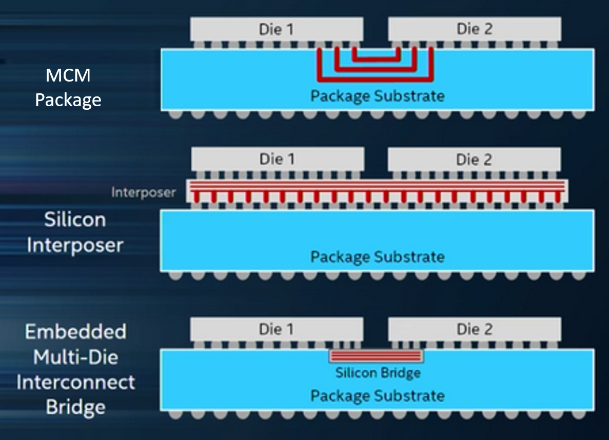
(Image courtesy ODSA)
For all of these, distances are small by PCB standards, and yet, even here, reach is a consideration. Millimeters matter. But we’re not talking just about physical interconnect here: we’re talking full protocol stacks, the upper layers of which would reside in firmware, with the lower layers being hardware.
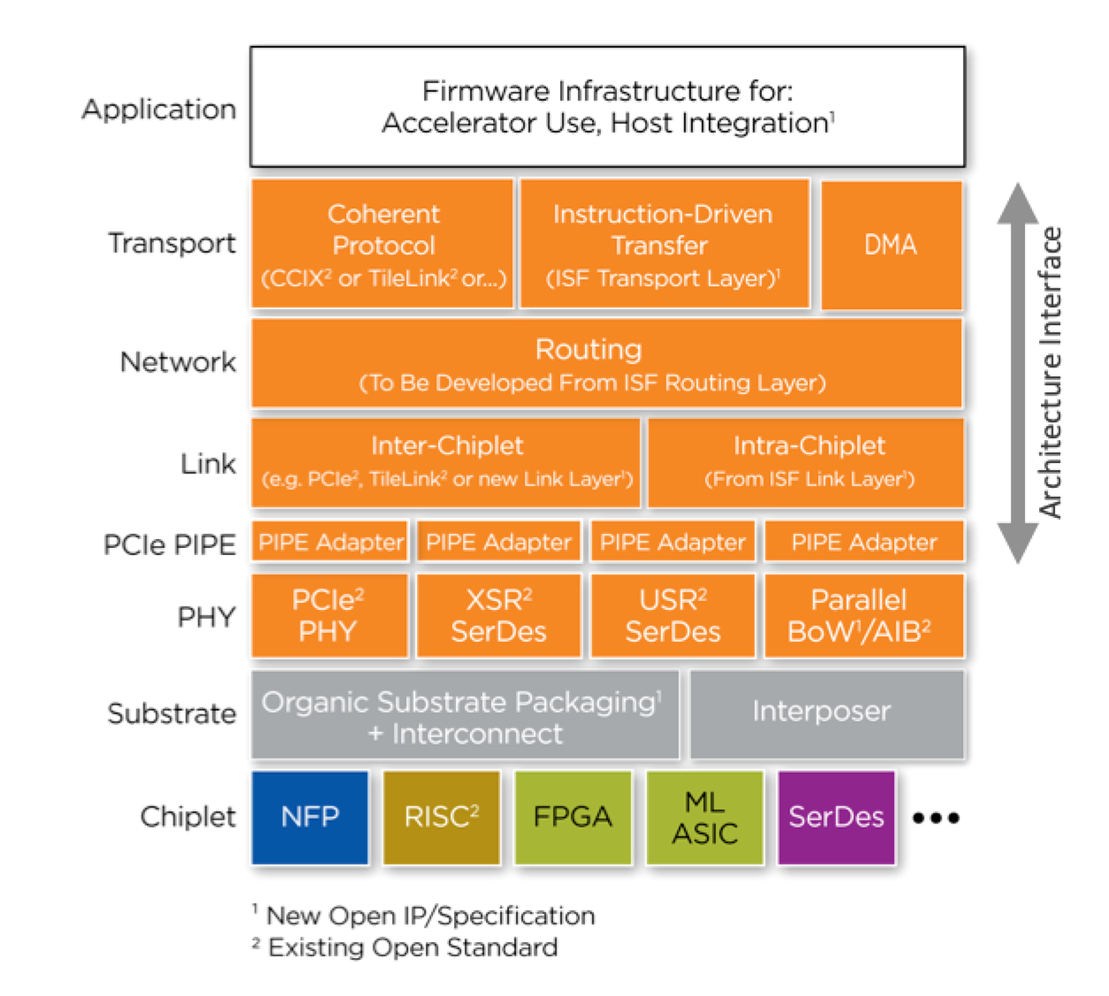
(Click to enlarge. Image courtesy ODSA)
You can see that the various layers call out different protocols – or call for a new protocol. Let’s walk through them to see what they are and where they came from. Some of them may be familiar. We’ll spend more time on the PHY alternatives after.
- CCIX: this is a coherency standard for use when connecting a CPU and an accelerator. It’s an extension to PCIe for chip-to-chip use. Rather than DMAing data to the accelerator, the CPU passes pointers.
- TileLink: This is a chip-scale interconnect protocol with multiple masters and slaves. It supports cache coherency as well. It comes from SiFive, but it’s not limited to RISC-V CPUs.
- ISF: This is developed by Netronome, an active participant in the ODSA project. They develop packet-processing solutions, not the least of which is an accelerator that they call a Flow Processor. In this context, ISF covers transport, routing, and link layers.
- PIPE: this is a part of PCIe, covering the interface between the MAC sublayer and the PHY layer.
For PHY interconnect, there are two fundamental options: serial and parallel. The first, and most obvious, option is the ubiquitous PCIe PHY. There are two other serial links in the image above, and their difference is their intended reach.
XSR is extra-short reach, for links up to 50 mm. USR is – you guessed it – ultra-short reach, for signals going no farther than 10 mm. (Yeah, they’re running out of superlatives… not sure what the next one will be called…). They both involve SERDES circuits using NRZ, PAM-4, or even Chord signaling. They’re specified by the Optical Internetworking Forum (OIF) for chip-to-chip and chip-to-optical connections. In the last OIF Common Electrical Interface (CEI) spec that I saw, both were positioned at 56 Gbps, DC coupled, with bit-error rates of 10-15. Presumably, USR will eventually reach higher bandwidths than XSR, since signals traverse a shorter distance.
Just to be clear on the signal formats, NRZ is your typical signal format – high is HI, low is LO, lasting for the duration of the symbol. We talked about PAM-4 not so long ago. Chord signaling is yet something different; it claims greater code efficiency than NRZ and better signal-integrity characteristics than PAM-4. It encodes n bits of data into n+1 physical bits. Honestly… I’ve looked into it a little bit, and it’s not so obvious how it works. So we’re going to need to come back to that one in the future if it starts to reach prime time.
For parallel interconnect, there are two options, both of which ODSA says require less sophisticated circuits than serial. You could even make them with 90-nm technology. First is BoW, which stands for “Bunch of Wires.” Yup, seriously. It has three modes:
- Basic, supporting up to 5 Gbps. It’s unterminated, with transmit and receive on separate lines.
- Fast, supporting up to 12 Gbps. It’s terminated, with transmit and receive on separate lines.
- Turbo, supporting up to 12 Gbps for both transmit and receive on the same wire – a total of 24 Gbps. So it’s full duplex. The receive circuits must subtract out the transmitted signal in order to recover the received signal (just like the telephones of yore).
AIB, meanwhile, is a recent addition. Originating at Intel, with support from DARPA, it can drive single-data-rate (SDR) signals to 1 Gbps and double-data-rate (DDR) signals to 2 Gbps. Yes, it’s not as fast as BoW at present, but, being newer, there may be more headroom.
The big difference between BoW and AIB is the intended substrate. BoW was conceived for organic substrates, and all testing and characterization results reflect that. AIB was intended for interposers or EMIB and can therefore handle many more signals spaced more closely together. The ODSA folks say that BoW might operate just fine in an interposer system as well, but there’s no data yet to support that.
Finally, there may be another entrant from AMD. Their Infinity architecture has an Infinity Fabric for On-Package (IFOP) option. Their materials say it’s for chip-to-chip interconnect, which I presume makes it also suitable for chiplet-to-chiplet interconnect. What I don’t know is if they intend to promote it as an alternative to the ODSA options. I attempted to contact them, but, as of “print” time, I have received no response. I’ll update if I get one.
Whichever options win out, having open standards will be the only way that a chiplet market can take flight.
More info:
Sourcing credit (all ODSA participants):
Bapi Vinnakota, Director of Silicon Architecture Program Management at Netronome
Bill Carter, CTO at OCP (Open Compute Project)
Quinn Jacobson, Strategic Architect at Achronix


What do you think of these chiplet-interconnect ideas?
Meanwhile, right about the time this was published, eSilicon made a related announcement:
https://www.eejournal.com/industry_news/esilicon-announces-availability-of-7nm-high-bandwidth-interconnect-hbi-phy-for-die-to-die-interconnects/