


Cobalt seems to be making an inexorable move into more and more applications as device features shrink. It’s largely been replacing tungsten in prior forays: for encapsulating copper and for high-aspect-ratio fill.
Well, cobalt now has a new target in its sights: copper interconnect. Yes, even venerable copper – which replaced aluminum somewhere around 20 years ago (IBM’s breakthrough was in 1997 – not even this century!). We’ll reprise some of the reasons why cobalt has been making inroads already, but then we’ll look particularly hard at why – and where – copper is at risk.
Melting the Grain
One of the big differences in how cobalt is handled is reflow. When it comes to replacing tungsten in the prior applications we saw, this has the immediate benefit of improving the quality of metal fill. Even if it deposits conformally, that’s undone by a reflow step that will eliminate any seams or voids in the fill.
In addition, when it comes to thin films, cobalt can also have lower resistance. That’s because the metal grain size is larger, making for smoother electron travel. The reason for the larger grains (at least partly) is that reflow step. It is, more or less, an anneal (as we’ll see), allowing grains to grow.
So… if that’s the case, then why not reflow tungsten and get the same benefits? Because tungsten is a refractory metal, meaning that it has a very high melting point – 3422 °C. Cobalt, on the other hand, melts at 1495 °C*. So it’s practical to reflow cobalt; tungsten… not so much.
Stacking up the Options
This time, we’re going to consider cobalt for interconnect. Applied Materials (“Applied” amongst friends) put together a comparison of tungsten, aluminum, copper, and cobalt. Notably, they made a distinction between narrow metal and wide metal features. So, for those of you silently asking the question, “Why now? What’s changed?” the answer is that feature size has changed.
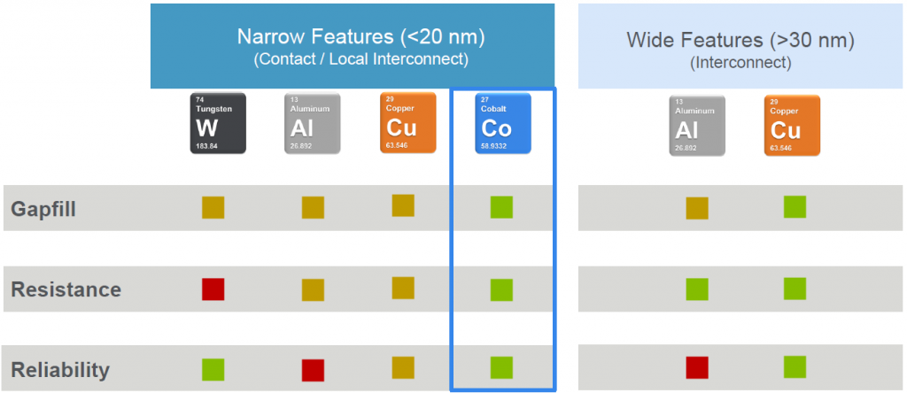
Let’s focus on narrow features. The ability to fill “gaps” – which gave us the high-aspect-ratio application – is highest with cobalt based on – surprise – reflow. Resistance is also lowest with cobalt, and reliability is high. That reliability thing largely relates to electromigration (EM).
EM hurts copper due to its melting point – 1085 °C. Aluminum is even worse, with a melting point of 660 °C. So, even though cobalt’s melting point – well below that of tungsten – helps from a reflow standpoint, it’s still high enough to beat copper and aluminum when it comes to EM.
But what about resistance? Before we dig into the wherefores there, let’s take a quick peek at the wide-feature numbers. (Applied’s boundary between narrow and wide is 20-30 nm.) Here they compare only aluminum and copper – the only metals to attain widespread use in interconnect. When it comes to resistance, copper gets a green box. On the narrow side, it gets only a yellow box. OK, those box colors aren’t exactly quantitative, but can we conclude that wide copper is less resistive than narrow copper?
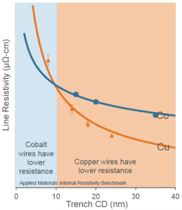
Well, that would be an obvious “Yes” if we were looking at resistance itself – anything wider is less resistive. But what if we’re looking at resistivity? (Which we are…) You’d think that this measure would factor out the whole dimension thing. But it’s still higher for narrower features. What’s up with that??
Here we get to the low-level notion of the mean free path of an electron. Applied has a graph of this metric for both copper and cobalt, as plotted against feature width. And lo, something unexpected happens: while copper dominates with wider features, there’s a crossover at around 10 nm. Above that, copper wins (and it looks like, with even wider lines, they become less sensitive to width – which sounds more intuitive). Below 10 nm, cobalt wins.
The Flow with Reflow
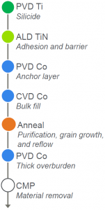
The cobalt interconnect flow is illustrated to the right. It probably looks familiar with the exception of that “anneal” step (which is where the reflow happens). In announcing this cobalt process, Applied is also introducing a new machine that performs this step: the Producer® Pyra™ Anneal machine. Deposition is done, as before, on the Endura® line; planarization is done on the Reflexion® LK Prime™ CMP Co machine.
While the Endura line does allow some integration, the “fill → anneal → overburden → planarization” flow involves FOUPs and moves each time (Endura → Producer → Endura → Reflexion)..
The overburden isn’t new to cobalt, but you might notice that it’s deposited after the anneal step – so that it isn’t annealed. Applied confirmed that the CVD fill slightly overfills the features, so all of the cobalt fill gets annealed. The overburden is applied with PVD, and they say that it’s a clean, pure film; so any of the overburden remaining after CMP should perform well along with the underlying annealed cobalt.
Presumably, if cobalt proves itself out in these applications, then, as dimensions continue to shrink, cobalt will move up the stack little by little. Will it ever take over all the way to the power grid? That’s tough to imagine… Power lines less than 10 nm wide sound sketchy. Then again, smarter people than I have made such obvious predictions before and been proven wrong. So it will be interesting to see just how far cobalt goes in this whole thing. Who knows… in a couple more years, we might be having this little chat again.
*Source: Applied Materials
All images courtesy Applied Materials
More info:
Applied Materials Cobalt Product Suite


What do you think of Applied’s tapping cobalt for interconnect?