

Ray Holt was a most unlikely candidate to develop a microprocessor chip set for the US Navy’s new F-14 variable-wing fighter jet. From an early age, Holt was a lackluster student, fully committed to a planned career as a professional baseball player. In 1962, as a senior at Dominguez High School in Compton, California, career counselors advised him not to go into engineering because he exhibited low mechanical aptitude. As a result, Holt ended up majoring in forestry at the University of Idaho. That move followed a year of working at a garbage dump after an unsuccessful semester at Compton Junior College when he dropped out. Unlikely beginnings, yet Holt ended up with a BSEE degree from Cal Poly in Pomona, California. He then joined Garrett AiResearch, presumably to design amplifiers. He didn’t like amplifiers much, and he never ended up designing one for Garrett.
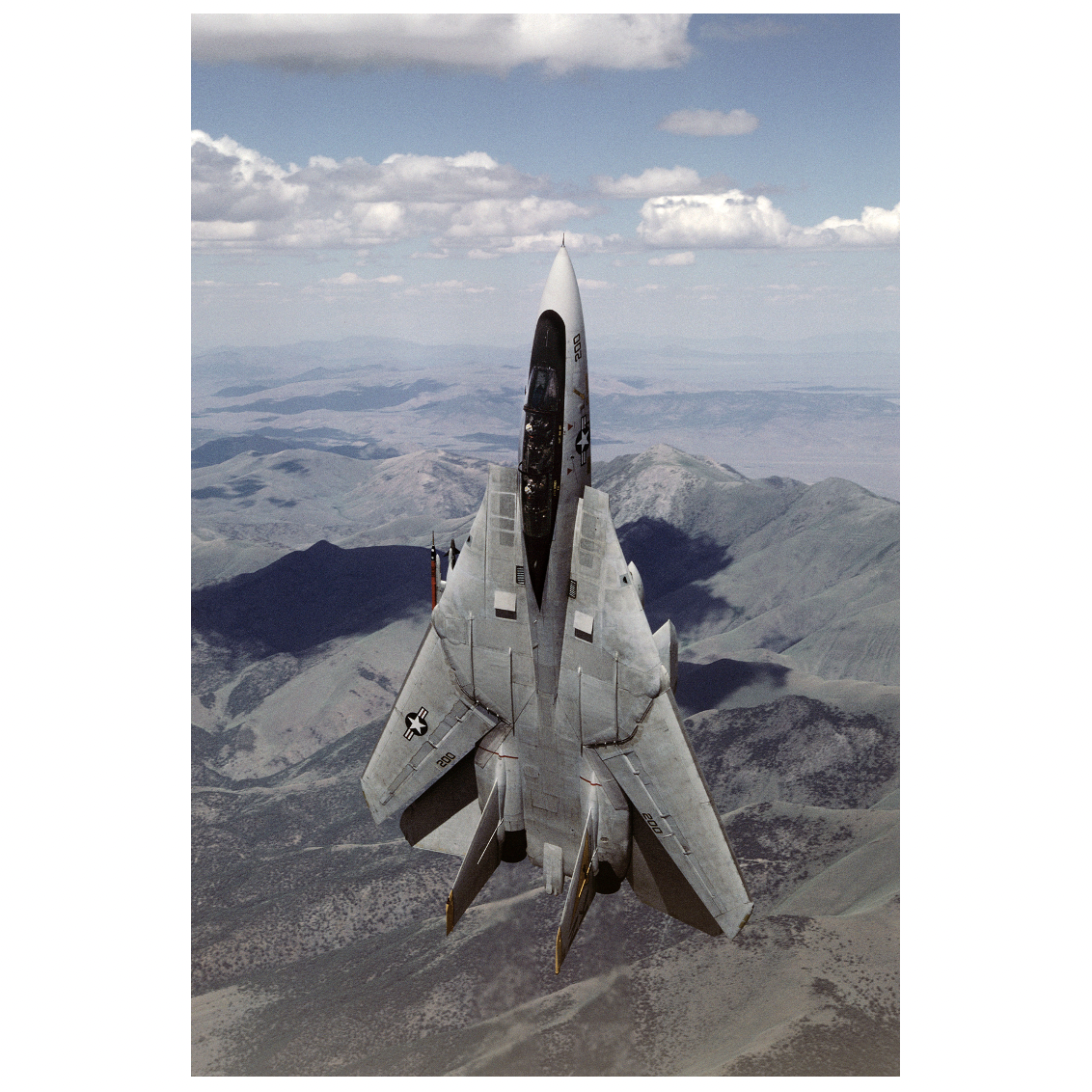
On his first day at Garrett, Holt was assigned to a team destined to design the CADC (Central Air Data Computer), the world’s first digital electronic flight computer, which would be installed in the US Navy’s F-14 Tomcat fighter. (If you’re not familiar with the F-14 aircraft, then I suggest you go watch “Top Gun,” which starred Tom Cruise. The F-14 is a co-star in that movie.)
Holt was picked for this team because he’d taken a class in logic design, which was one more class than anyone else on the team had attended. He worked on the CADC project from 1968 through 1970, when the F-14 first flew. His design work overlaps other microprocessor development projects, most notably the Four Phase Systems AL1 byte-slice chip set and the Intel 4004 4-bit microprocessor. Neither the CADC, aka the MP944, nor the AL1 can be considered single-chip microprocessors because they require multiple chips to implement the fundamental components of a microprocessor: an ALU, a program counter, an instruction-fetch mechanism, an instruction decoder, and a bus interface.
I can easily argue that the Intel 4004 also doesn’t qualify as a single-chip microprocessor because it required a double handful of additional TTL parts to build a working system, but the 4004 does incorporate all the fundamental components named in the previous paragraph. Declaring the 4004 as the first commercial microprocessor is fairly well recognized canon at this point and I feel no need to rehash this topic because I thoroughly discussed these three microprocessor chips and chipsets back in 2018 in an article titled “Will We Ever Really Know Who Invented the Microprocessor?” and again late last year in an article titled “Which Was The First Microprocessor?” The purpose of this article is to make you aware of Holt’s short, self-published book, “The Accidental Engineer,” which he wrote in collaboration with Italian engineer, technology author, and journalist Leo Sorge. (However, if you relish arguing which was the first microprocessor, I invite you to log in and opine in the comment section below.)
Holt’s book is short, only 80 pages long, and it’s clearly a labor of love. It’s a bit rough around the edges, grammatically speaking, but if you enjoy reading about the history of little-known technology projects, then you’ll definitely enjoy this book for the intimate look into a consequential project that it provides. Imagine becoming a principal engineer on the team that brought military flight computers from the mechanical age to the digital electronic age in one giant leap and not being able to discuss the highly classified project for another three decades, all while watching from the sidelines as microprocessors blanketed the earth and wormed their way into nearly every technology niche. It must have been frustrating. It must have been excruciating!
It’s worthwhile diving into the design of the CADC to compare it with what we consider to be a conventional microprocessor. Before we do that, I need to remind you of the state of semiconductor art in 1968. This period marked the very beginning of the MOS LSI epoch. The densest process technology of the day was P-channel MOS (P-MOS) and the “next big thing” in semiconductors back then was calculator chips. Everyone was designing them.
It’s not surprising that Holt narrowed down the field of potential manufacturers for the CADC chipset to American Microsystems (AMI), Rockwell Semiconductor, and General Instruments (GI). All three of these semiconductor makers were involved in P-MOS chip development at the tail end of the 1960s. AMI helped Garrett design the CADC chips, so it was the front runner for getting a production contract.
Although any of these three semiconductor makers could have produced the CADC chipset, none of them seemed to want the contract because of the low production volumes. Grumman eventually built 712 F-14 fighter jets, so the entire order for all CADC ICs initially would be only a few hundred a month, or just a few thousand parts spread over the projected decades-long lifetime of a military aircraft. That total volume, a few thousand parts, was little more than a one-month production order for one calculator chip, so the economics didn’t favor this business even though the manufacturers would make far more money per unit for the CADC ICs. According to Holt’s book, Garrett AiResearch ultimately had to invest heavily in AMI stock before the company would agree to manufacture the CADC chips.
The CADC was designed to be an embedded computer from the start. It incorporated a variety of sensor inputs including air pressure, air temperature, and pilot control settings to generate control signals that operated the aircraft’s variable-wing geometry and control surface actuators and to provide signals to the fighter aircraft’s precision ordnance systems.
Part of the overall CADC project involved the development of special 20-bit ADCs that could digitize the analog outputs of the custom-built air pressure sensors to achieve the required 1-foot altitude resolution at 80,000 feet. That’s another huge achievement for the day, but not part of Holt’s main story. However, it does mean that the CADC had to perform polynomial math on sensor data using a 20-bit, signed, fixed-point format. To achieve the needed calculation speed while operating under the constraints of the relatively slow P-MOS chips’ maximum clock speed, the CADC design team developed a parallel architecture that split the calculations into three streams and distributed each stream separately to the 20-bit multiplier, divider, and binary-operations chips. There was no assembler or compiler for the CADC. You programmed it directly in machine code.
In all, the CADC team developed six main chips, including:
- A Parallel Multiplier Unit (PMU)
- A Parallel Divide Unit (PDU)
- A Special Logic Function (SLF), which performed binary logical and branching operations
- The Data Steering Logic Unit (SL), basically a serial data multiplexer
- Random Access Storage (RAS), what we’d call a register bank or a RAM today
- Read-Only Memory Unit, a 2560-bit ROM with integrated program/data counter
These chips move data over external serial buses to save package pins and to reduce board space, but that meant that a 20-bit word transfer required 20 clock periods, at 2.66 microseconds per clock. The ROM chip is organized as 128 20-bit words and has an integral program/data counter. The RAS chip is organized as sixteen 20-bit registers and accepts a 5-bit address/instruction word with four bits to specify the targeted register and the fifth bit specifying whether a write is to occur. These specialized ROMs and RAMs conceptually resemble the specialized RAM and ROM chips that Intel developed for the 4004 microprocessor during the same period. In both cases, the specialized nature and organization of these memories is somewhat removed from today’s more general RAMs and ROMs.
Modular functional partitioning allowed the CADC team to fit complex mathematical function units into the limited transistor counts available on the LSI P-MOS chips of the day while building an embedded computer with three parallel, computational pipelines. The CADC used 28 of these chips: one PMU, one PDU, one SLF, three SLs, three RAS devices, and nineteen ROMs.
Each of the three computational pipelines has its own control module, built with ROMs, for data and instruction sequencing, and the three control modules are controlled by an executive unit, built with more ROMs. This sophisticated architecture lies somewhere between a complex state machine and a microprocessor. It hints of and predates VLIW machines and modern microprocessors with multiple execution units. Unfortunately, the CADC stayed secret for the next 30 years and did not affect mainstream microprocessor evolution. Instead, it seems several of the innovations designed into the CADC were independently developed later by others. How might things have developed differently if the CADC had not remained under wraps for three decades?
Holt left Garrett in 1971 and joined AMI, the semiconductor maker that eventually did manufacture the CADC ICs. While there, he worked on the development of two proprietary and obscure AMI microprocessor architectures: the 3-chip 7200 and the microprogrammable, 2-chip 7300. AMI then decided there was no future in microprocessors and disbanded its microprocessor group. Holt became a microprocessor system consultant and developed the JOLT line of 6502-based microprocessor boards, which was later bought by Synertek and then quickly became part of Honeywell. Holt also published the “Microcomputer Digest,” an early microprocessor newsletter, and he started a very early software distribution company. These days, you’ll find Holt in rural Mississippi, igniting the imaginations of underserved kids using computers and robotics. His is a remarkable engineering career, never far from the main development path that electronics has taken over the last half century.
If you’d like to learn more about the remarkable Ray Holt, head over to his Web site, https://firstmicroprocessor.com/. While you’re there, why not purchase a copy of his book?


