


Generally speaking, I tend to duck when someone lobs a business-related press release in my direction. Call me a techno-weenie if you will, but I really don’t care to learn that Company A has been pondering the possibility of potentially signing a letter of intent with Company B to establish a framework within which to commence discussions about the prospect of collaborating on some vaguely defined project at some undefined time in the future.
I would say that I have an unwritten rule (the best kind, in my experience) about this sort of thing. On the other hand, “rules are meant to be broken,” as they say, although I personally prefer the adage, “rules are for the obedience of fools and the guidance of the wise.”
To cut a long story short (which is opposite to the way my dear old mother taught me to do things), I didn’t run for the hills when my old friend Kalyn Kolek emailed me to say, “I’m now on the venture capital (VC) side of things at Anzu Partners. I’m working with a new startup called EnCharge AI that my firm has invested in and that I think will be of interest to you.”
Kalyn then proceeded to tempt me with three teasing bullet points as follows:
- EnCharge’s technology was developed at Princeton University and is led by a world-class, multi-disciplinary founding team from Meta, NVIDIA, Qualcomm, and IBM.
- This charge-based in-memory computing technology has demonstrated AI performance with orders-of-magnitude higher compute efficiency and density than has been achieved by best-in-class digital accelerators, such as GPUs or TPUs, resulting in over 150 TOPS/W for 8-bit compute.
- EnCharge will deliver platforms that provide over 20x higher performance per watt and over 14x higher performance per dollar, compared to the best-in-class digital AI accelerators.
I couldn’t help myself. I was lost when I saw “150 TOPS/W.” I simply had to look at the press release, EnCharge AI Launches With $21.7M Series A to Enable Edge AI at Scale, which—in addition to the information summarized above—informed me that “EnCharge offers a software stack that supports broad AI models and resolutions while integrating seamlessly into user frameworks and design flows” and “EnCharge seeks to unlock the immense potential of AI by making it accessible to power-, energy-, and space-constrained applications at the edge. These capabilities are valuable for market applications such as automotive sensing, advanced manufacturing, smart retail, smart warehouses and logistics, industrial robotics, and drones.”
I also bounced over to the EnCharge website to learn more about the company and its founders, Naveen Verma, PhD (CEO), Kailash Gopalakrishnan, PhD (CPO), and Echere Iroaga, PhD (COO). “Among them, these three guys boast a cornucopia of business and technology know-how sufficient to make a success of anything they turn their hands to.” (said Max, BSc)
Kalyn had succeeded. I wanted to learn more, so we set up a video chat between your humble narrator (I pride myself on my humility), Naveen, and Echere, while poor old Kailash was left to run the company in their absence.
We got off to a great start:
Me: “Hmmm. Your company is called EnCharge and I’m informed you have developed a charge-based in-memory computing technology. Can I assume this is based on a floating-gate memory technology like Flash?”
Naveen: “No”
This wasn’t as bad as it sounds because Naveen smiled as he imparted this nugget of knowledge. Before we proceed, I should perhaps note that I’ve been introduced to several analog-based artificial intelligence (AI) and machine learning (ML) accelerators based on floating-gate memory technologies over the past year or so.
A racing summary of the concept behind those technologies in a crunchy nutshell is as follows. AI and ML are based on artificial neural networks (ANNs). These involve layer upon layer of artificial neurons. They also involve eye-watering amounts of matrix manipulations and computations. In fact, 95% to 99% of an AI/ML application is devoted to these matrix operations. At the core of these matrix operations are multiply-accumulates, where the results of a bunch of multiplications are accumulated.
We can do all this digitally using a regular microcontroller unit (MCU), but this is time-consuming and power-gobbling to say the least. Alternatively, we can do things in a massively parallel fashion using FPGAs, or we can employ a hybrid approach using arrays of small processing cores in the form of graphics processing units (GPUs). In fact, FPGA and GPU-based solutions largely dominate this space in data centers. However, as we move closer to the edge (where the internet meets the real world), size, cost, and power consumption considerations become increasingly important.
I always think of floating gates in the context of simple Flash memory devices, where each cell (gate) can essentially hold a 0 or a 1 value. However, some companies have developed the ability to control the number of electrons in the floating gate to represent 256 different values (equivalent to 8 bits of storage) (see also Meet Mythic AI’s Soon-to-be-Legendary Analog AI). If these values are used to represent a weight (coefficient) in an ANN, then each Flash cell can be used to perform an analog multiplication (voltage x conductance) between its activation voltage and its coefficient. The currents from all of the Flash cells in a column are additive (an analog addition), which means we can think of each Flash cell as acting like a synapse and each column of cells as representing a neuron.
On the one hand, analog computation is inherently less precise than its digital counterpart. On the other hand, AI and ML are inherently probabilistic in nature. What this means is that it really doesn’t matter if an AI reports a 96% probability it’s looking at a chicken or a 97% probability it’s looking at a chicken… Either way, we are pretty darned sure that we have a chicken-centric scenario on our hands.
NOW SIT UP AND PAY ATTENTION! This is the clever bit. Naveen noted that “things get messy” when you use semiconductor devices to perform your analog compute. This is because semiconductor-based analog elements are sensitive to environmental conditions like temperature fluctuations and process variations in the form of material parameters. As a result, Flash-based analog-centric technologies require constant monitoring, tweaking, and re-calibration. We can think of this as adding lots of analog-to-digital-to-analog micro-loops. Since much of this is performed using digital techniques, it sort of detracts from the advantages of using analog in the first place.
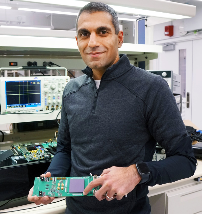
Naveen Verma, Co-Founder and CEO of EnCharge AI, holds a prototype of the company’s advanced computing technology in his laboratory at Princeton University.
The solution developed by EnCharge AI is to steer away from employing the chip’s semiconductor substrate to implement the analog elements used to perform the matrix multiply-accumulate operations, and instead create incredibly precise capacitors out of metal wires, which are essentially free when creating a chip in CMOS technology. These capacitors are not sensitive to temperature or semiconductor process variations; they are sensitive only to structure and geometry, which can be well-controlled in CMOS.
Imagine a column of these capacitor cells. Remember that Q = CV, which means the charge Q on each cell (wire capacitor) is the product (multiplication) of its capacitance C and applied voltage V. The total charge of the column is additive, which gives us our accumulation. Once again, we can think of each cell as acting like a synapse and each column of cells as representing a neuron.
Let’s see how well I can explain what happens next. (Don’t think of this as me being too lazy to draw a diagram. Rather, think of it as an exercise in visualization to build your mental muscles. It’s just one more service I offer. You’re welcome.) We start with an array of these cells that’s thousands of rows and hundreds of columns in size. This is called a compute-in-memory array (CIMA). This array has associated digital computation and dataflow buffers, a programmable digital SIMD engine, and some control logic, all of which are collectively known as a compute-in-memory unit (CIMU).
The reason everything needs to be programmable is that different AI/ML models have different requirements. Some layers may be performing 3×3 convolutions, some may need to implement 9×9 convolutions, others may wish to realize dilated convolutions, and so forth.
Now imagine an array of these CIMUs all connected by an on-chip network (OCN). This super-array is what’s known as a scalable in-memory computing (IMC) neural-network (NN) accelerator. I think of this as an IMCNNA, but I don’t think this terminology is employed by the guys and gals at EnCharge.
We haven’t finished yet. What we are talking about is a CMOS chip that, in addition to the IMCNNA, also includes a cluster of standard Arm processor cores that are used to perform on-chip pre- and post-processing housekeeping tasks, a PCIe Gen 5 interface to communicate with a higher-level host processing system, and a bunch of other stuff.
One huge aspect of all this is the fact that EnCharge technology is based on standard CMOS manufacturing processes, which means it can be implemented at the latest and greatest process nodes (they started at 65nm, migrated to 28nm, and are currently at 16nm).
Do you remember earlier when we said, “EnCharge offers a software stack that supports broad AI models and resolutions while integrating seamlessly into user frameworks and design flows.” What this means is that users can take AI/ML models created using standard design frameworks (PyTorch, TensorFlow, ONNX…) running on conventional FPGA/GPU-based systems, and quickly and easily start accelerating these models using EnCharge’s IMCNNA (scalable in-memory computing neural-network accelerator… I know… this doesn’t roll off the tongue… we need to come up with a better name).
In summary, the chaps and chapesses at EnCharge are pursuing an edge-to-cloud strategy. Their target is outside the data centers, close to the edge, but not at the extreme edge. They are aiming at big automation tasks that need to run state-of-the art AI/ML models, including industrial, smart manufacturing, smart retail, warehouse logistics, robotics, etc.
The folks at EnCharge say that their charge-based in-memory computing technology has demonstrated AI performance with orders-of-magnitude higher compute efficiency and density than has been achieved by best-in-class digital accelerators, such as GPUs or TPUs, and that their current proven-in-silicon solution achieves 150 TOPS/watt.
I for one am tremendously excited. Once again, this is a technology implementation I didn’t see coming and I can’t wait to see where it ends up going. How about you? Do you have any thoughts you’d care to share?


All extremely exciting! Mythic’s work also seems very exciting. I can think of the perfect application for this technology. I wonder if the folks at EnCharge or Mythic would like to support an educational nonprofit 🙂
theboom.org
You can but ask them (make sure you let them know that you heard about them here on EEJournal.com 🙂
Unfortunately the future is uncertain for Mythic as they seemed to have stopped operating due to lack of funds.
That’s sad, but it’s the fate of many small companies — I hope they do get more funding and become a success — I thought their technology was really interesting.