


I recently had a very interesting chat with Steven Woo, who is a Fellow and Distinguished Inventor at Rambus. I’d like to kick off by saying that Steven is a delight to talk to. He’s obviously got a size-16 brain (one of the sporty models with “go-faster” stripes on the side), but he’s so good he ends up making you feel clever (as opposed to so many people who make me feel like an… I was going to say “ignoramus,” but I don’t know how to spell it).
That reminds me of a joke I heard on the radio on the way into work this morning. A young lad is calling his mom saying, “Remember how my teacher said I’d never be any good at poetry because I’m dyslexic? Well, I just made two candlestick holders and a vase, and they look great!”
I’m sorry. It’s been a long day. (I can’t help myself. Just saying this reminds me of John Cleese saying “I’m sorry, I have a cold” in the classic Monty Python Dead Parrot sketch. In turn, mentioning John’s name reminds me of the time the two of us dined on an ice cream delight — see Sharing an Ice Cream Sundae with John Cleese).
But we digress… As you may or may not be aware, Rambus Incorporated is an American technology company that was founded in 1990 and that currently specializes in chip interface technologies and architectures. However, the purpose of my chat with Steven was not to talk about Rambus per se, but rather for him to bring me up to date with what’s happening in memory space. We started by considering how things have evolved over the years.
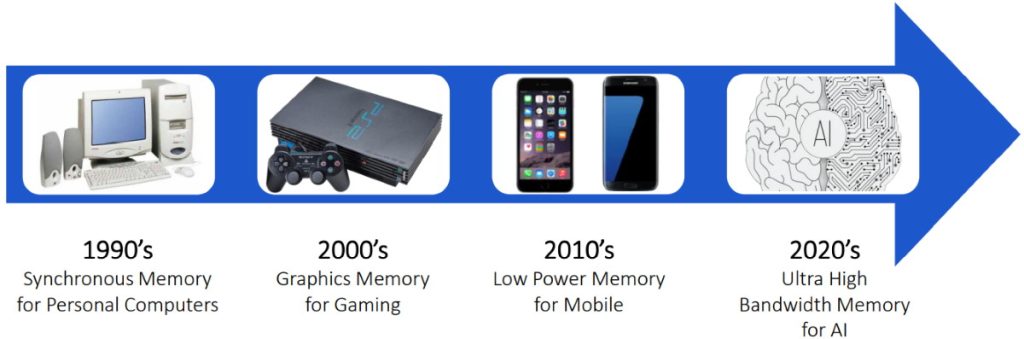
Advances in computing drive new memory technologies (Image source: Rambus)
If you look at the past few decades, each has been somewhat defined by a classic paradigm in computing. In the 1990s, it was all about the rise in personal computers. This was accompanied by the development of synchronous dynamic random-access memory (SDRAM), which is the generic name for any form of DRAM in which the operation of its external pin interface is coordinated by an externally applied clock signal (by comparison, the DRAM chips produced from the early 1970s to the early 1990s employed an asynchronous interface). The original SDRAMs were classed as single data rate (SDR).
Personal computing continued to grow in the 2000s. These years saw the development of the first double data rate (DDR) SDRAMs, which are retroactively referred to as DDR1. In the same timeframe, Rambus’s main claim to fame, as far as most folks were concerned, was its invention of Rambus DRAM (RDRAM). At one stage, Rambus memory technology was expected to become the standard in PC memory but… you know how it is… stuff happens. Over time, Rambus transitioned into a company that designs, develops, and licenses chip interface technologies and architectures that are used in a wide range of digital electronics products.
DDR1 (2001-2005) was superseded by DDR2 (2006-2010), DDR3 (2011-2015), DDR4 (2016-2020), and now DDR5 (2021-). The 2000s also saw the growth of more visual computing in terms of graphics and gaming. In turn, this led to the introduction of Graphics DDR (GDDR) SDRAM, which is specifically designed to satisfy the requirements of graphics processing units (GPUs) (see also What the FAQ are CPUs, MPUs, MCUs, and GPUs?).
Although cloud computing had been around for a while, the 2010s saw an exponential growth in this area, with a corresponding demand for vast quantities of high-performance memory. The 2010s also experienced exponential growth in mobile devices, with a corresponding need for significant amounts of low-power memory.
Although we are still only at the beginning of the 2020s, we can already tell that what’s really driving memory is artificial intelligence (AI), including machine learning (ML) and deep learning (DL) (see also What the FAQ are AI, ANNs, ML, DL, and DNNs?). Steven says that he’s seeing a lot of interest in extreme performance with respect to memory and chip-to-chip solutions; also, that there doesn’t seem to be any end in sight, especially in the AI domain. As Steven puts it: “This is really putting quite a lot of interesting pressure on memory capacity and performance and power efficiency.”
As an aside, do you realize that we are now more than 1/5th of the way through the 21st Century? Also, it won’t be long before the terms “the 20s,” “the 30s,” and so on are understood by younger folks to refer to the 2020s and 2030s, not the 1920s and 1930s as is the case with curmudgeonly codgers like your humble narrator.
Returning to AI, the thing that’s really taken a lot of people by surprise is the rapid growth in size of neural network (NN) models and training sets, which means we’ve got to keep growing memory capacity, bandwidth, and power efficiency. As Naveen Rao (VP and GM, AI Products Group, Intel) said, speaking at Intel’s AI Summit in 2019 (which already seems like a lifetime ago): “The number of parameters in a neural network model is actually increasing on the order of 10x year on year… and outpaces basically every technology transition I’ve ever seen.”
As an example, OpenAI Generative Pre-trained Transformer 3 (GPT-3) was introduced in May 2020 and was in beta testing as of July 2020. Part of a trend in natural language processing (NLP), GPT-3 is an autoregressive language model that uses deep learning to produce human-like text. The point of interest here is that the full version of GPT-3 has a capacity of 175 billion ML parameters. Even more scary, models with over a trillion parameters are on the horizon.
People are using a variety of techniques to extend the memory capacity and bandwidth that’s currently available — like using reduced precision math, pruning, and quantization — but these are just stopgap measures because we need more of everything (capacity, efficiency, bandwidth, security).
As is usually the case, there are so many cool technological things going on that it makes your head spin. Common memory systems for AI applications include on-chip memory, high bandwidth memory (HBM), and GDDR memory.
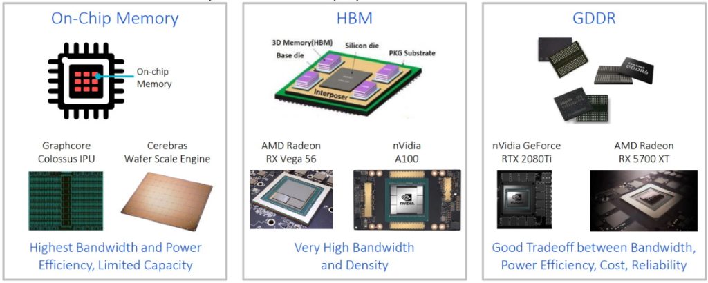
Common memory systems for AI applications (Image source: Rambus)
Not surprisingly, on-chip memory offers the highest bandwidth and power efficiency, but it’s limited in its capacity. At the time of this writing, with a standard reticule-sized die, we can achieve only a few hundred megabytes of capacity, albeit at an extreme bandwidth. Even in the case of the wafer-scale engine (WSE) from Cerebras in which an entire wafer is employed as a single compute engine, the first generation of this engine boasted only 18 GB of on-chip SRAM, which is less than a few HBM DRAMs.
With respect to HBM, this refers to stacks of up to eight DDR SDRAM dice along with an optional base die that can include buffer circuitry and test logic. One or more HBM stacks can be connected to memory controllers on the main processing element (CPU, GPU, FPGA) via a common substrate like a silicon interposer — or mounted directly on top or underneath the main processing element — with the processor-HBM combo being presented as a system-in-package (SiP).
When it comes to external memories, the current mainstream offerings are the latest incarnations of DDR and GDDR, which have been around for a couple of decades and use more traditional manufacturing techniques. In the case of AI applications, GDDR in particular offers a good middle ground for designers who don’t have the necessary expertise to use more technologically aggressive technologies or who can’t tolerate the cost of HBM.
Another aspect to all of this is the way in which external memories are connected to processors like CPUs (and GPUs and FPGAs, of course). There are several interesting developments in this area as are illustrated below.
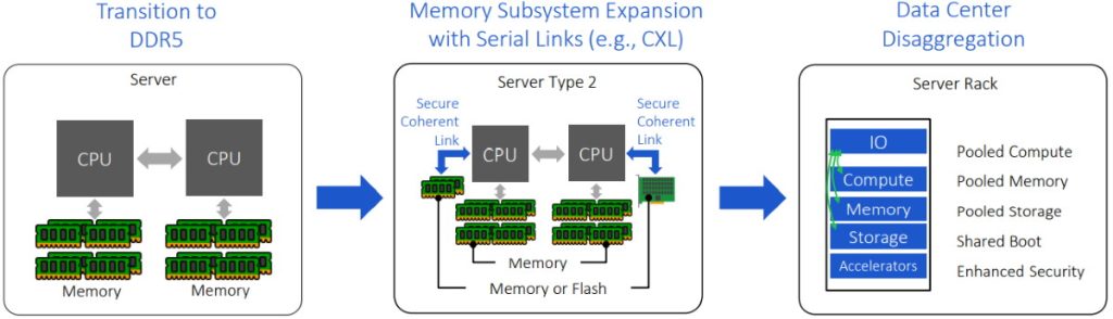
New memory technologies are delivering increased capacity and bandwidth and improved total cost of ownership (TCO) (Image source: Rambus)
The first of these developments is the transition from DDR4 to DDR5, which only just started, and which will ramp up rapidly during 2022. With greater capacity, higher bandwidth, and better power efficiency
than its DDR4 predecessor, DDR5 will follow the traditional DDR form factor; that is, it will be presented on dual in-line memory modules (DIMMs) that plug into DIM sockets on the motherboard, where these sockets are connected directly to the CPU(s).
As an example, the latest generation of Intel desktop processors, codenamed Alder Lake (see Will Intel’s New Architectural Advances Define the Next Decade of Computing?), support both DDR4 and DDR5. The first members of this new family were released on 4 November 2021, which is just five days ago as I pen these words. Meanwhile, Rambus is offering DDR5 interface devices for use by the vendors who create memory sticks, and memory stick vendors like Crucial by Micron are offering DDR5 solutions for use with Alder Lake-based systems (it’s like the circle of life).
Another technology that will be making its debut in platforms next year — and that will really start to take off in the market a year or two after that — is an industry-supported cache-coherent interconnect for processors, memory expansion, and hardware accelerators called compute express link (CXL). Based on the Peripheral Component Interconnect Express (PCIe) standard, CXL will allow systems to access even higher capacity and bandwidth memory subsystems.
Once we start thinking about moving memory outside of DIMM sockets, the next step is to think about moving it outside the server cabinets in data centers. This is part of the current trend toward disaggregation, in which data centers have cabinets containing only processors, other cabinets containing only memory, and yet more cabinets containing only storage. We can think of this as having pools of resources. The idea here is that when jobs come in, they simply grab as much of each resource as they require. When a job’s done, it releases these resources back into their respective pools from whence they can be provisioned to future jobs in different ratios.
There’s so much more to all of this that it makes my head spin. For example, the upcoming family of server processors from Intel, codenamed Sapphire Rapids (again, see Will Intel’s New Architectural Advances Define the Next Decade of Computing?), will boast the interesting ability to have memory attached to the processor that can act as a cache or as actual memory. This provides an interesting flexibility — so interesting, in fact, that the industry may be experimenting with it for some time while we figure out just what to do with it.
The bottom line is that AI is currently a major driver in the semiconductor domain in general, and in the memory realm in particular. Having memories with greater capacity, higher bandwidth, and lower power consumption is critical for future progress in AI. As Steven says, “There are multiple paths going forward, and this is keeping us on our toes. This is a neat time, because memory is a focus and there’s an opportunity to do some really interesting innovation moving forward.”
Prior to my conversation with Steven, if you’d caught me in an elevator and asked me what Rambus does, my knee jerk reaction would be to waffle on about their old RDRAM technology, but they’ve moved on since then. Their current focus is memory interface chips, high-speed interface IP, and security IP. You have only to look at the Products Page on their website to see the wealth of offerings they… well, offer.
In fact, the history of Rambus is interesting, complicated, and varied. It can be defined from what one can glean from the internet, but there are many misunderstandings, and there’s a much more coherent story to be told. Steven has been with Rambus from the earliest days of the company to where they are now. He says that there are good business reasons for why they moved in the directions they did; also, that there are good reasons why the industry took the paths it did. Happily, we had a follow-up conversation where all was revealed, and I shall be communicating this in a future column.
But wait, there’s more! I commenced this column by saying that the purpose of my chat with Steven was not to talk about Rambus per se, but rather for him to bring me up to date with what’s happening in memory space. However, I feel it would be churlish of me to not at least mention the fact that several Rambus-related announcements have crossed my desk since our original conversation, including the following:
- Rambus Advances Server Memory Performance with the Industry’s First 5600 MT/s DDR5 Registering Clock Driver
- Rambus Delivers CXL 2.0 Controller with Industry-leading Zero-Latency IDE
- NextChip Selects Rambus Security IP to Secure Apache6 Automotive Processor
I’d better stop here before I think of something else that I want to say. Let’s hand things over to you — what do you think about all of this?


