


I’m sure you know what the terms CPU, MPU, MCU, and GPU stand for. I’d wager you think you know which functional blocks each of these terms embraces. But are you 100% certain? Would you bet on it?
One of the problems we have in the electronics and computing industries is a surfeit of TLAs (three letter acronyms). The fact that the same TLA can be used to represent multiple and diverse things only exacerbates the matter.
Another issue is the fact that we tend to learn a lot of things by osmosis, gradually (often unconsciously) assimilating nuggets of knowledge into a conceptual framework that appears to make sense… until it doesn’t.
I just had a quick Google while no one was looking. I was trying to track a saying down. Instead, I ended up falling down a Google rabbit hole with topics like:
- You Don’t Know What You Don’t Know
- The More You Know the More You Realize You Don’t Know
- How Do You Know What You Don’t Know You Don’t Know?
- The Value of Knowing What You Don’t Know You Don’t Know
There were also a couple of self-help columns that side-tracked me for a while:
Unfortunately, none of these articles was what I was looking for, although they did provide some interesting reading. I vaguely remember hearing that it’s only when you try to teach something to someone that you discover the gaps in your own knowledge; that is, the things you don’t know. I’m sure this can be found as a pithy proverb, adage, aphorism, or apothegm that was first stated by someone famous deep in the mists of time, but I cannot track it down to save my life.
Having said this, Art Markman summed things up nicely in his Do You Know What You Don’t Know? column when he spake as follows:
Find an object you use daily (a zipper, a toilet, a stereo speaker) and try to describe the particulars of how it works. You’re likely to discover unexpected gaps in your knowledge. In psychology, we call this cognitive barrier the “illusion of explanatory” depth. It means you think you fully understand something that you actually don’t.
Yes! The illusion of explanatory depth. That’s just what I was going to say — and it’s certainly something I will be saying in the future to anyone who doesn’t get out of the way fast enough — but it’s Art’s next point that is particularly pertinent to our discussions here:
We see this every day in buzz words. Though we often use these words, their meanings are usually unclear. They mask gaps in our knowledge, serving as placeholders that gloss concepts we don’t fully understand.
And thus we wend our weary way to the point of this column (yes, of course there’s a point), which is that a lot of people think they know what the terms CPU, MPU, MCU, and GPU embrace, but they may not know as much as they think they know.
Take a moment to imagine that you are about to walk into a room of people with limited engineering knowledge. Your assignment will be to sketch things out on a whiteboard and explain how terms like CPU, MPU, MCU, and GPU relate to each other. How confident are you that you would be up to the task?
ALUs and CPUs
I’ve been thinking about this quite a lot recently, and the following is how I would go about explaining things. At the heart of a computer is a functional block called the arithmetic logic unit (ALU). Not surprisingly, this is where arithmetic and logical operations are performed, like arithmetically adding two numbers or logically ANDing two values.

The arithmetic logic unit (ALU) is the heart of a computer
(Image source: Max Maxfield)
Note that I didn’t use an arbitrary shape for the ALU — this ‘Y’ form is the symbol engineers always use because the ALU accepts two input values and returns a single output.
When we combine the ALU with a bunch of registers (see also Registers vs. Latches vs. Flip-Flops), some instruction logic, some addressing logic, and some control logic, we end up with a central processing unit (CPU). Note that when we say “logic” in this context, we are talking about the primitive logic gates and register elements used to form digital electronic systems.
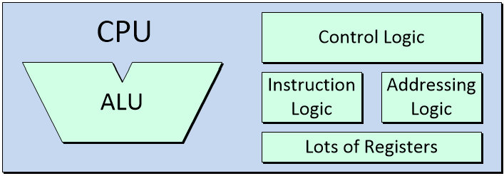
The central processing unit (CPU) is the brain of a computer
(Image source: Max Maxfield)
The CPU is in charge of executing the instructions forming a computer program by performing the arithmetic, logic, control, and input/output (I/O) operations specified by those instructions.
Memory and Alternative CPU-Memory Architectures
In order for the CPU to perform its magic, it requires access to memory subsystems that are used to store instructions and data. This is where things get a little tricky, because there are two fundamental computer architectures called the von Neumann (or Princeton) architecture and the Harvard architecture.
In the case of the von Neumann/Princeton architecture, both the data and the instructions are stored in the same physical memory space and accessed using the same address, data, and control busses. By comparison, in the case of the Harvard architecture, the instructions and data are stored in physically distinct memory devices and accessed using their own busses.
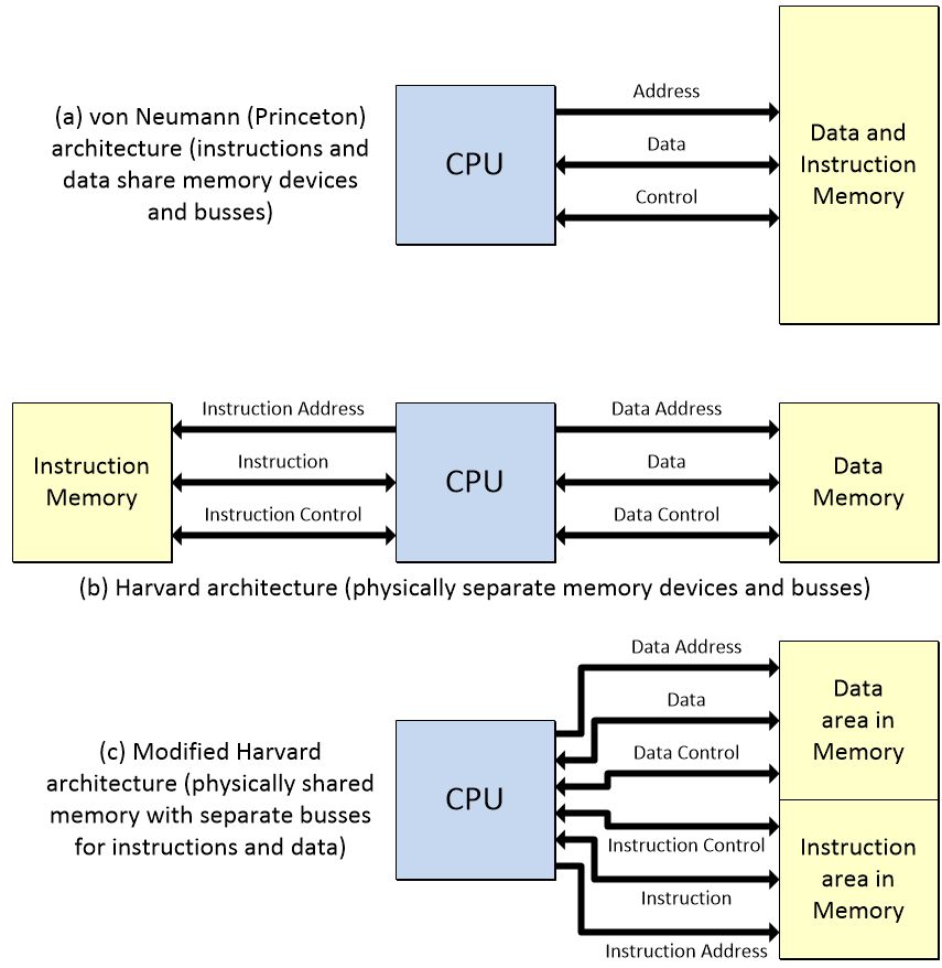
Fundamental computer architectures: von Neumann/Princeton, Harvard, and Modified Harvard (Image source: Max Maxfield – click to enlarge)
There’s also a flavor called a “modified Harvard architecture,” in which the instructions and data share the same physical memory devices but are accessed using their own busses (special mechanisms prevent instructions from being mistaken for data, and vice versa).
For the remainder of our discussions here, we will focus on the von Neumann/Princeton architecture (because it’s easier for me to draw), but everything we talk about is applicable to all three architectural alternatives.
Got Cache?
One problem with computers is that it takes a relatively long time for instructions and data to pass back and forth between the main memory and the CPU. The thing is that the vast majority of programs involve lots and lots of small loops in which the same actions are performed over and over again. The solution is to create a (relatively) small, high-speed memory called the cache, along with a special cache controller, which is located close to the CPU, and which keeps a copy of frequently accessed instructions and data.
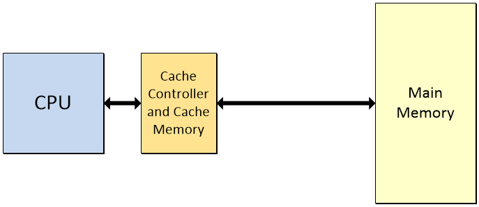
The cache is a (relatively) small, high-speed memory located close to the CPU (Image source: Max Maxfield)
Note that the above diagram is a gross simplification. Modern CPUs have separate caches for instructions and data. Also, there is a hierarchy of caches called L1, L2, L3, etc. (where ‘L’ stands for “Level”). The L1 cache is the smallest, fastest, and closest to the CPU.
One problem system designers have to consider is ensuring that any changes the CPU makes to the contents of the cache are subsequently reflected in the main memory (if it’s appropriate to do so). Synchronizing the contents of the caches and main memory while maintaining the integrity of those contents is an eye-wateringly complex task, so you’ll be delighted to discover that we won’t discuss it any further here.
One thing we do have to mention, however, is the topic of cache coherency, which rears its ugly head in systems that boast multiple CPUs — each with their own cache subsystems — sharing a common memory resource.
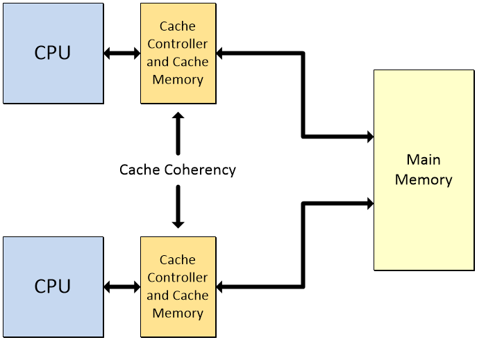
Problems can arise when multiple CPUs share a common memory resource (Image source: Max Maxfield)
As the Wikipedia tells us: “In a shared memory multiprocessor system with a separate cache memory for each processor, it is possible to have many copies of shared data: one copy in the main memory and one in the local cache of each processor that requested it. When one of the copies of data is changed, the other copies must reflect that change. Cache coherence is the discipline that ensures that the changes in the values of shared operands (data) are propagated throughout the system in a timely fashion.” I couldn’t have said it better myself.
Adding an FPU
Early CPUs performed integer multiplication operations using repeated addition. They also performed integer division operations using techniques that are too complicated to go into here (see also How Computers Do Math). It wasn’t long before designers began to add special multiplier/divider functions.
Similarly, many early CPUs were architected to perform fixed-point arithmetic operations. When it came to more complex floating-point operations, these were realized by breaking things up into sequences of simpler operations and using the fixed-point architecture to perform these operations.
As people started to use computers more and more, they wanted their computers to run faster and faster, and one way to achieve this was to add a special floating-point unit (FPU). The FPU’s role is to carry out addition, subtraction, multiplication, division, square root, and bit-shifting operations on floating-point values.
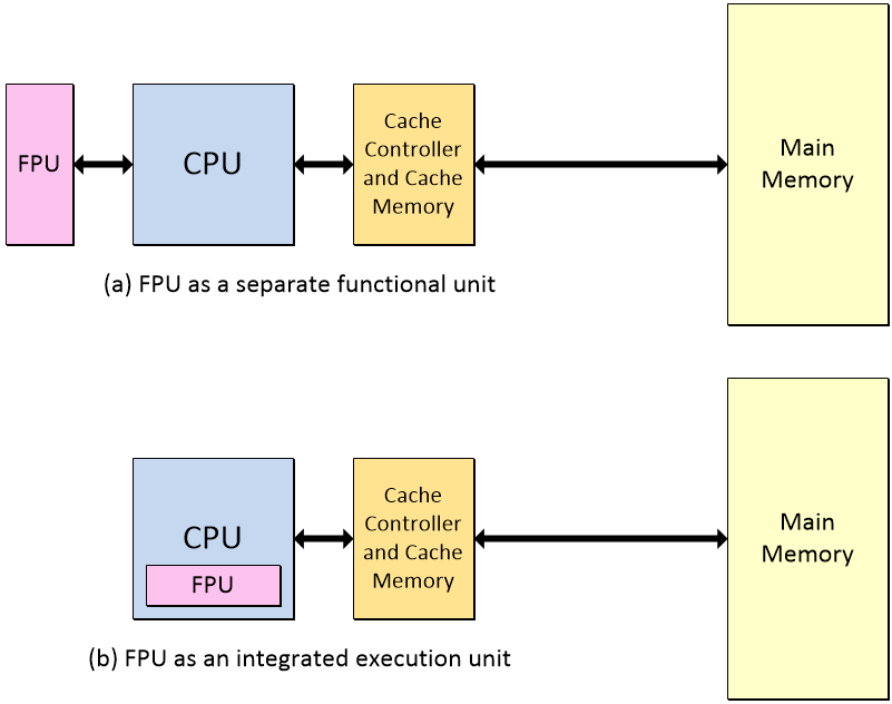
The FPU carries out operations on floating-point numbers
(Image source: Max Maxfield – click to enlarge)
It is very common for the FPU to be implemented as a separate functional unit, but it is also not uncommon for one or more FPUs to be integrated as special execution units within the CPU.
Memory Protection and Management: MPUs and MMUs
A memory protection unit (MPU) allows privileged software — such as the operating system (OS) — to define regions in the memory and to assign access permissions and attributes to those regions.
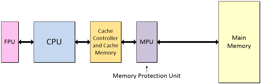
Adding a memory protection unit (MPU) (Image source: Max Maxfeld)
The MPU monitors transactions between the CPU and the memory and raises the alarm (triggers a fault exception) when an access violation is detected. The main purpose of the MPU is to prevent a program from accessing memory that has not been allocated to it. This prevents an innocent bug in a regular program or a malicious malware program from affecting other processes or the operating system itself.
The next step up the hierarchy is to use a memory management unit (MMU), which augments the functions of a memory protection unit (MPU) with additional capabilities.
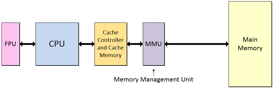
Upgrading the memory protection unit to a memory management unit (MMU) (Image source: Max Maxfield)
This is where things start to get a little tricky. The simplest level is to run a single program on a “bare machine” (colloquially referred to as “bare metal”), which refers to the computer executing programs directly on the CPU without an intervening operating system. In this case, the programs can be compiled using absolute (physical) addresses.
More sophisticated systems run a special program called an operating system (OS). The OS allows the user to run multiple programs at the same time. Consider your own personal computer, for example, on which you might have your word processor, graphics, and email programs all running concurrently. The way this works is for these programs to be compiled using relative addressing. The MMU’s task is to translate the virtual addresses in the programs to physical addresses in the main memory.
Note that, since MMUs subsume the functions of MPUs, they are mutually exclusive — a system may have one or the other (or neither) but not both.
Microprocessors and Microcontrollers
When we use the term “computer” these days, the majority of people (non-engineers) typically think of their tower, laptop, notepad, or tablet machines. By comparison, depending on their domain, engineers may think of workstations or servers, or they may think of microprocessors and microcontrollers.
Before we start talking about microprocessors and microcontrollers, however, we should note that all of the concepts discussed above apply to computer architectures generically. For example, early computers circa the 1960s consisted of rooms full of large cabinets called “mainframes.” Each cabinet contained a different function, like the CPU or the main memory. Colloquially, computers of this ilk were referred to as “big iron” machines.
The first CPUs to be implemented as integrated circuits (“silicon chips”) circa the 1970s were referred to as microprocessors (µPs). Later, they started to be referred to as microprocessor/microprocessing units (MPUs). These days, µP and MPU are taken to be synonymous.
The early MPUs contained only the CPU. Functions like a floating-point unit (FPU), which was also known as a math co-processor, and a memory protection unit (MPU) or memory management unit (MMU) were implemented on separate devices, all of which were mounted close together on the printed circuit board.
Of course, having the three-letter acronym MPU stand for both microprocessor unit and memory protection unit only adds to the fun and frivolity, but you can usually work out what someone is talking about from the context of the conversation (if not, ask them to spell things out before you put any money on the table).
These days, there are thousands of MPU offerings. Some contain only a solitary CPU, some contain a CPU along with various combinations of cache, FPU, and memory protection or memory management units, and some contain multiple CPUs, FPUs, etc. (Note that MPUs may contain additional functions — we are focusing on core functionality for the purposes of these discussions.)
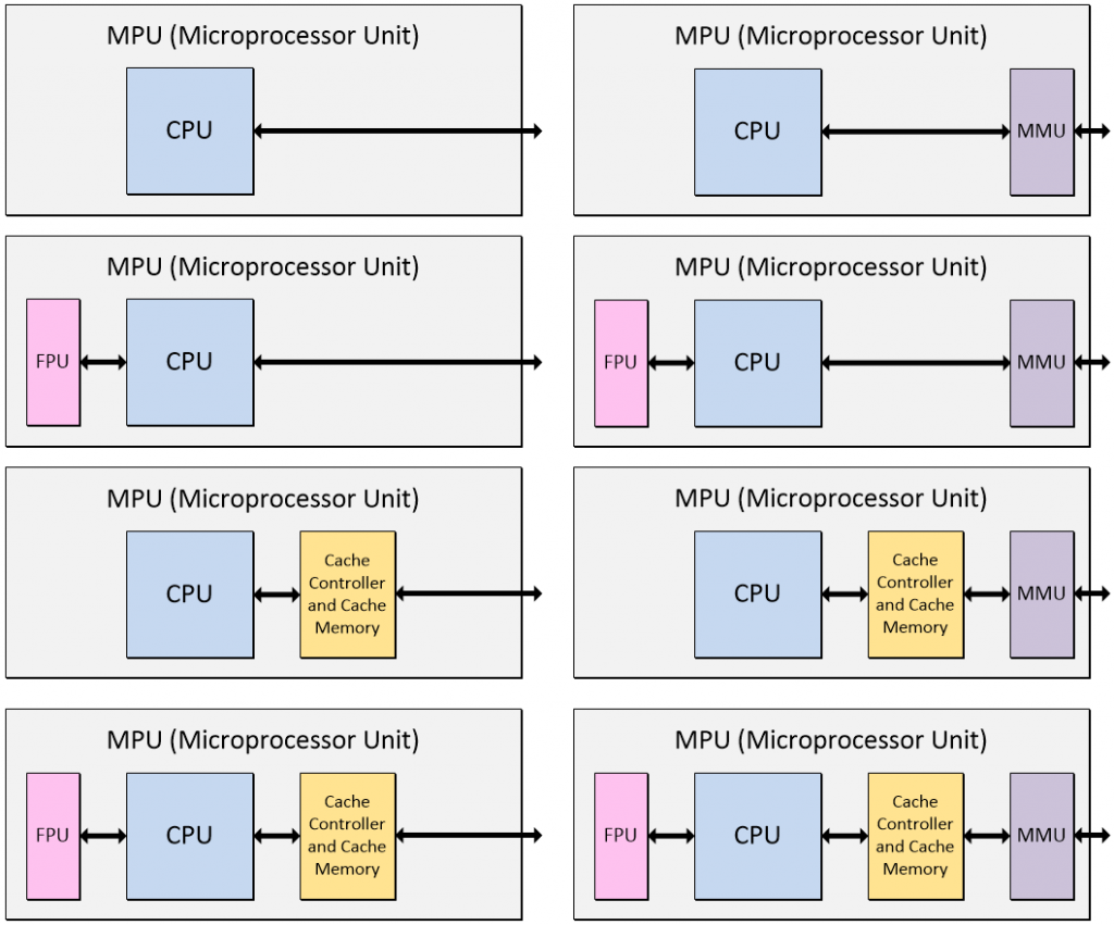
Microprocessor units (MPUs) come in many shapes, sizes, and configurations (Image source: Max Maxfield)
As opposed to a memory management unit (MMU), some microprocessor units (MPUs) may contain a memory protection unit (MPU), but we’ve not shown these variants here to avoid confusion. Also, as a rule of thumb, it’s more common to find a memory management unit in a microprocessor and a memory protection unit in a microcontroller as discussed below.
One of the distinguishing features of a microprocessor is that it doesn’t contain any memory (excluding any cache). That is, all of its memory is provided external to the device. By comparison, a microcontroller (µC) — also known as a microcontroller unit (MCU) — does contain memory comprising both non-volatile program memory (NVM) in the form of Flash and volatile working memory in the form of SRAM. An MCU will typically contain a variety of additional functions and capabilities, including counters and timers and analog inputs with analog-to-digital converters (ADCs).
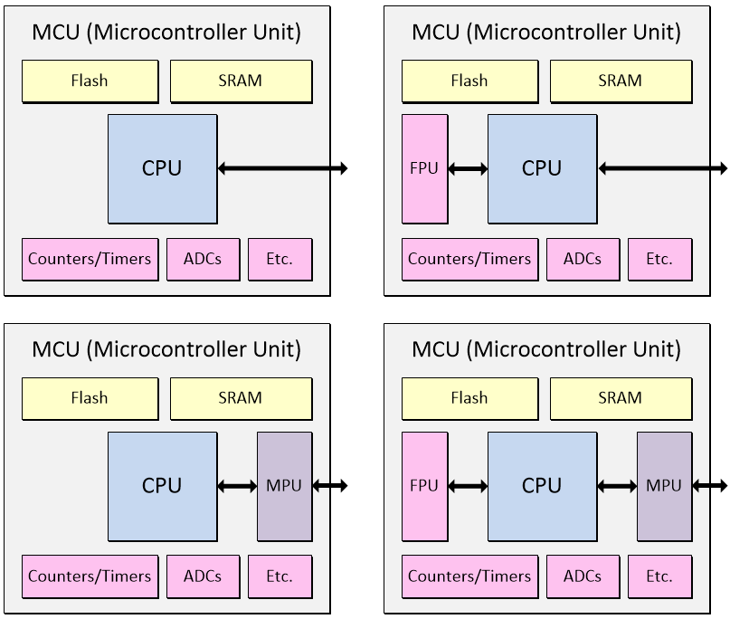
Microcontroller units (MCUs) come in many shapes, sizes, and configurations (Image source: Max Maxfield)
One reason MCUs typically don’t contain any cache memory is that they often have to provide real-time control functionality and performance. This may involve the program running “bare metal” — or under a kernel or real-time operating system (RTOS) — and having a cache memory subsystem tends to kill determinism.
Furthermore, MCUs are typically not running complex operating systems like Linux or Unix, and so do not require a memory management unit (MMU). If they have any memory protection at all, it will typically be no more complex than a memory protection unit (MPU). Once again, MCUs may contain additional functions — we are focusing on core functionality for the purposes of these discussions.
Graphics Processing Units (GPUs)
Last, but not least, for this column, we come to graphics processing units (GPUs). While a microprocessor unit (MPU) will contain only a few (e.g., one, two, four, or eight), sophisticated CPU cores, a GPU can contain hundreds or thousands of simpler CPU cores, each with a small amount of local memory, and FPU, etc.
As their moniker would suggest, GPUs were originally intended for graphics applications, in which the same operations need to be performed on hundreds of thousands or millions of pixels on a screen. However, GPUs also find use in applications that benefit from massively parallel processing, including hardware acceleration, cybercurrency (“Bitcoin”) mining, and high-performance computing (HPC).
MPU (microprocessor) and GPU combos are found in systems like mobile phones, laptop, notepad and tablet computers, workstations, and gaming consoles. Meanwhile, MCU (microcontroller) and GPU combos may be found in embedded systems.
OK, that’s it for this column. As always, I welcome any comments, questions, and suggestions. Until next time, have a good one!


Nice diagrams, Max! I’ll be look forward to how you describe GPU architectures. 🙂
Thanks for your kind words — especially re my diagrams — speaking of which, did you see my FPGA diagram in this column (https://medium.com/supplyframe-hardware/mcu-designers-intro-to-fpga-hardware-34f613a74291)? I must admit I went to town on that one.
Re GPUs, these architectures are pretty propitiatory — the ones I really knew in depth were a few years ago — I’ll have to think about this — maybe if I get to chat with the folks at NVIDIA — are there any particular architectures you have in mind?
Excellent, evoked memories of my days as a software engineer writing operating systems, 1100 OS. I wonder why you did not even mention the RISC architecture?
Ah, good point — maybe I should have mentioned RISC and CISC — it’s only after you’ve posted the column that you think of these things (or, in this case, YOU thought of it LOL)