


A few days ago at the time of this writing, the crème de la crème of the world’s technical press were welcomed to an invitation-only virtual event that many people would have given their eye teeth to experience — Intel’s Architecture Day 2021.
Due to some strange oversight on somebody’s part (or possibly because I have friends in low places), I was summoned to join these distinguished journalists and attend this august occasion (my mother is so proud — she will be “dining out” at the hairdressers for weeks on this, regaling her friends with tortuous tales of my derring-do).
In a moment I’m going to delight you with details of some amazing architectural innovations that will blow your socks off (you may want to take a few moments to ensure that you are suitably attired). Seriously, I have news to impart regarding architectural advances whose ramifications will reverberate down the years that are to come. First, however, let’s take a moment to reflect on how this all started deep in the mists of time — 50 years ago as I pen these words — when I was a bright-eyed, bushy-tailed 14-year-old lad building my first brainwave amplifier (one day I hope to get it working). [Cue “travelling back through time” music and accompanying visual effects.]
The first commercially produced microprocessor was the Intel 4004, which was launched in 1971. This little scamp was presented as a 16-pin device. It had a 4-bit data bus and a 12-bit address bus. Since the package was so pin-limited, eight pins were employed to multiplex the address and data busses, with the remaining pins used to provide power and ground, reset/test triggering, two clock inputs, and handshaking with the ROM and RAM memory devices. Containing approximately 2,300 transistors, the 4004 could execute 60,000 operations per second.
As an aside, I have one of these little beauties in my own collection (mine is a ceramic C4004 variant without the grey traces in the ceramic).
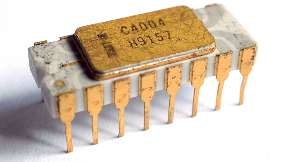
Intel 4004 microprocessor (Image source: Thomas Nguyen/Wikipedia)
As I wrote on the DIY Calculator support site: “In November 1972, Intel introduced the 8008, which was essentially an 8-bit version of the 4004. The 8008 contained approximately 3,300 transistors and was the first microprocessor to be supported by a high-level language compiler called PL/M. The 8008 was followed by the 4040, which extended the 4004’s capabilities by adding logical and compare instructions and by supporting subroutine nesting using a small internal stack. However, the 4004, 4040, and 8008 were all designed for specific applications, and it was not until April 1974 that Intel presented the first true general-purpose microprocessor, the 8080. This 8-bit device, which contained around 4,500 transistors and could perform 200,000 operations per second, was destined for fame as the central processor of many of the early home computers.”
In 1978, Intel introduced the 16-bit 8086, which gave rise to what is now known as the x86 family of instruction set architectures (ISAs).
We could waffle on about the evolution of Intel’s devices for hours, but we have other fish to fry (which reminds me that it would be remiss of me if I failed to point out that I was recently interviewed on Amelia Dalton’s Special Edition: Makers Today! Fish Fry Podcast).
However, we digress… Returning to Intel’s Architecture Day 2021, I was blown away by everything I saw and heard. The meaty part of the presentation commenced with Raja Koduri — who is the senior vice president and general manager of the Accelerated Computing Systems and Graphics (AXG) Group — explaining how technology is changing the world, how having access to enormous computing power is becoming crucial to almost every aspect of our lives, how high-end users are asking for their workloads to run 1,000x faster by 2025, and how Intel is positioned to achieve this goal.
There’s a huge amount to wrap one’s brain around here, so I’m going to introduce things at a 30,000-foot level to show how everything fits together, after which we will talk about nitty-gritty facts and figures.
New x86 Cores
We start with the introduction of two new x86 cores that will lay the foundation for what is to come. First, we have the Efficient x86 Core, which — for those who keep their ears to the ground — was previously code-named “Gracemont.” This was designed from the ground up to be a scalable microarchitecture that can address computing needs across a wide spectrum of products, from low-power mobile applications to many-core microservices. Although it’s being billed as the world’s most power-efficient x86 core, this little beauty still manages to deliver more instructions per clock (IPC) than Intel’s most prolific core to date.
Next, we have the Performance x86 Core, which was previously code-named “Golden Cove.” While still maintaining high efficiency, this core was designed for raw speed, pushing the limits of low latency and single-threaded application performance, all while providing a scalable architecture to serve a wide range of platforms from laptops to desktops to data centers.
Intel Thread Director Technology
In computer science, a “thread” is the smallest sequence of programmed instructions that can be managed independently by a scheduler, which is typically a part of the operating system. Suppose we have a processor that is comprised of multiple cores, such as a cluster of the Efficient x86 and Performance x86 cores we just discussed. How do we assign threads to these cores to seamlessly maximize performance and efficiency?
The conventional approach is to assign threads to cores based on static rules, but this leaves performance on the table and creates an overhead for software development. The problem is that things are constantly changing, especially when multiple applications are running at the same time, where each application can have multiple threads. Some of these threads will be mission-critical, while others will be associated with mundane background tasks. Some threads will lean to vector operations, which are better served by Performance Cores, while other threads may predominantly contain scalar operations, which can be addressed by Efficient Cores. The thing is that what a thread is doing may vary back and forth over time — sometimes mostly vector, other times predominantly scaler, and so forth.
The answer is Intel Thread Director Technology. This provides hardware monitoring of what each thread is currently doing and passes this information to the operating system (OS), which can decide how to handle things. All of this happens dynamically and autonomously, thereby providing a significant performance boost to existing applications (this is on top of the performance boost provided by the new cores) without any changes having to be made to the software. The combination of Efficient Cores, Performance Cores, and Thread Director provides a huge impact on user-perceived performance and power consumption. Even better, Intel has been working with Microsoft to integrate this functionality into the forthcoming Windows 11 release.
Alder Lake Client SoC
The first of Intel’s next-generation processors to feature the combination of the new Efficient Cores, Performance Cores, and Thread Director technology is code-named Alder Lake.
Built on the Intel 7 process, Alder Lake’s compute fabric can support up to 1,000 gigabytes per second (GBps), which is 100 GBps per core or per cluster and connects the cores and graphics through the last level cache to the memory. Speaking of which, the memory fabric can deliver up to 204 GBps of data and dynamically scale its bus width and speed to support multiple operating points for high bandwidth, low latency, or low power. To complement all of this, the I/O fabric supports up to 64 GBps, connecting the different types of I/Os as well as internal devices and can change speed seamlessly without interfering with a device’s normal operation, selecting the fabric speed to match the required amount of data transfer.
Xe-HPG, Xe-Core, Xe-SS, and the Alchemist SoC
This is where things start to get complicated (at least, for your humble narrator). Did you know that there are currently 1.5 billion PC gamers in the world, and this number is increasing in leaps and bounds?
That’s not the complicated bit, of course — I just thought we’d start with something we can all understand. The real trick here is to wrap your brain around all of the abbreviations that I’m about to hurl your way. First, we have Xe-HPG, which is a new discrete graphics microarchitecture designed to scale to enthusiast-class performance for gaming and content creation workloads (I’m assuming HPG stands for “High Performance Graphics,” but it could also refer to “High Performance Gamer”). This microarchitecture features the scalable Xe-core; the more cores you have, the higher your graphics performance.
The first discrete graphics chips to boast these technologies is the Alchemist family of SoCs (where Alchemist was formerly known as DG2). The client roadmap includes the Alchemist, Battlemage, Celestial, and Druid SoCs, all of which will come to market under the Intel Arc brand.
One thing that really caught my attention was Intel’s new neural-based super sampling technology called Xe-SS. The way I understand this is that — given a choice — we would all like our games to be rendered at 4K resolution, but this is mind-blowingly computationally expensive and can result in lower frame rates. As a result, a lot of gaming solutions render at a resolution of 1080p and then upscale to 4K, but traditional upscaling solutions result in visual artifacts and loss of fidelity. By comparison, Xe-SS uses a neural network and artificial intelligence to perform its upscaling. This allows the application to render in 1080p at higher frame rates and for the rendered frames to be upscaled on the fly with such fidelity that there’s no visible quality loss as compared to rendering in native 4K.
To be honest, this has to be seen to be believed, so I’m delighted to be able to tell you that Intel has uploaded a video of this portion of Architecture Day to YouTube (the cool graphics start at time 7:25, but I’d strongly recommend watching the whole thing).
I can’t believe that I’ve already written so much while covering so little. All we’ve talked about thus far relates to client computers like those found in mobile devices, laptops, and desktops, but there’s so much more…
Welcome to the Data Center
The second half of Architecture Day was focused on the data center. Kicking this off was a presentation on Intel’s next-generation Xeon scalable processor, whose code name is Sapphire Rapids. In addition to the Performance x86 cores we talked about earlier, Sapphire Rapids boasts new accelerator cores, a new memory architecture, a new fabric architecture, a new I/O architecture, a host of new software and security features, and… the list goes on.
Next, we were introduced to a suite of FPGA-based infrastructure processing units (IPUs), which are programmable networking devices designed to enable cloud and communication service providers to reduce overhead and free up CPU performance. All of these IPUs were interesting, but the real eye-opener was Intel’s first ASIC IPU, which is called Mount Evans.
Have you ever heard the expression, “Saving the best for last?” Well, that’s what the little scamps at Intel did, because the final device they introduced was a GPU called Ponte Vecchio that is targeted at applications like artificial intelligence and high-performance computing (HPC). With more than 100 billion transistors (I have to keep re-reading this to convince myself that I’ve not made a mistake), this device is a beast. In fact, it’s composed of 47 active tiles (think silicon die) implemented using five different process nodes, all seamlessly connected together to look like a single gigantic die. Actually, this is not quite true, because it also involves 3D die stacking, the daunting details of which will make your brains leak out of your ears.
Rather than me trying to explain all of this here, let’s take a look at this Ponte Vecchio video snippet (when I say “snippet,” I should point out that it’s a 25-minute snippet) that explains everything in exhilarating detail.
Earlier, I promised nitty-gritty facts and figures, and I like to think I’m a man of my word, but there are simply too many numbers for me to throw around here, so let me instead guide you to this Fact Sheet from the Intel Newsroom.
To be honest, I’ve barely scraped the surface here. Each of these architectural advances — the Efficient x86 core, the Performance X86 core, Thread Director, Alder Lake, Alchemist (including Xe-HPG, Xe-Core, and Xe-SS), Sapphire Rapids, Mount Evans, and Ponte Vecchio — demands a column in its own right. Happily, my chum and colleague Steve Leibson has started the ball rolling with a column on IPUs in general and Mount Evans in particular here on EEjournal.com (see Ooh, Ooh that Smell! Can Intel’s IPUs Clean up the Cloud Data Center Mess?).
All I can say is that my mind has been well and truly boggled by everything I saw at Intel’s Architecture Day 2021. In many cases I was flabbergasted. In some cases — like Ponte Vecchio — I think it’s fair to say that my flabber has never before been quite so gasted. I cannot wait to see the devices based on these new architectures hitting the market (I’m already lusting after an Alder Lake-powered laptop computer). How about you? Do you have any thoughts you’d care to share on anything you’ve seen here?


modular ALU’s that execute exactly as per design ?….the end of unmarked dark alleyways ?….the mind fizzes…
I’m not sure about “fizzes” — but I know mine has been boggled — I find it hard to wrap my brain around the complexity — of for the days of the simple 8-bit microprocessor LOL
Same old smoke and mirrors. Intel invented multi-core and threw it over the wall to let the world figure out how to program it. Well, multithreading is not a general purpose performance booster either, but it opens the door to more complexity.
Branch prediction, out of order. superscalar nonsense goes back to CDC and IBM360 model 91 when programs were written in assembler. Cache was invented for matrix inversion IBM 370 model 85 programmed in assembler. I would like to see how 3 levels of cache were justified. I know “It is intuitively
obvious”… nonsense!
Microsoft put FPGAs in the data center after they found that FPGAs can out perform super scalar running at 10 times clock frequency higher than FPGA. see “Where’s the beef” research paper.
No one has figured out a way to show that pipeline latency does not impact performance. Ignore it and it will go away….
Now that Intel is in the FPGA business, it seems that they could devote some resource to make FPGA design easier, instead they go off on this tangent. They know that “complexity is what sells” as Professor Dijkstra
said.
And he went on to invent the “Shuntingyard Algorithm” which is at the heart of today’s compilers.
Say what you will, but I for one was impressed by what I heard — I’m looking forward to seeing the new processors based on these technologies.