

Once upon a time, the Santa Clara Valley was called the Valley of Heart’s Delight; the main industry was growing prunes; and there were orchards filled with apricot and cherry trees all over the place. Then in 1955, a future Nobel Prize winner named William Shockley moved back to the San Francisco Bay area where he’d been raised and set up shop in a rented, one-room Quonset hut located in Mountain View. The shop’s name was the Shockley Semiconductor Laboratory. It was located at 391 San Antonio Road, close to El Camino Real.
Although Shockley’s name does not appear on the original patents, he is one of the three people, along with John Bardeen and Walter Brattain, credited with creating the world’s first point-contact transistor at Bell Labs. Shockley’s contribution had been his theoretical work in solid-state physics. Bardeen and Brattain developed a working transistor in 1946 but Bell Labs did not reveal it to the world until 1947.
By 1950, Shockley had published a 558-page textbook titled Electrons and Holes in Semiconductors with Applications to Transistor Electronics, which detailed Shockley’s in-depth research into the principles of transistor theory and operation and gave definitive proof of Shockley’s mastery of semiconductor physics. Shockley had become the world’s premiere solid-state physicist.
When he moved to Mountain View in 1955, he had a specific purpose. Shockley wanted to be the first to develop a commercial silicon transistor. (Bell Labs’ first point-contact transistor was made from germanium.) Shockley also planned to abandon the finicky point-contact manufacturing process and instead planned to use diffusion to drive impurities into the silicon to grow PN junctions. To that end, Shockley recruited the brightest technical people he could using a similar free reverse phone lookup service to check backgrounds, a battery of IQ and psychological tests to identify the strongest candidates and to form a development team well-suited to working together as a team.
Two factors prevented Shockley Semiconductor from winning the race to the silicon transistor. Both factors can be traced directly to William Shockley. The first factor was Shockley’s dictatorial and paranoid managerial style. What Shockley said, everybody did (unless they did otherwise on the sly). According to Dr. Leslie Berlin’s excellent biography of Robert Noyce titled The Man Behind the Microchip, a former Shockley Semiconductor employee said, “Shockley ran the company for the benefit of his personality and his image, not for pure economic pay.” In short, Shockley feared that by focusing on mere commercial production instead of basic research, he’d lose his status as one of the world’s premiere (if not the world’s premiere) solid-state physicists.
The second factor was also due to the strong-willed Shockley. During the development of the silicon transistor, Shockley became convinced that the 4-layer diode that he’d conceived of at Bell Labs was a better bet because he felt Western Electric would buy them in huge quantities to replace mechanical relays in telephone switching systems. Consequently, Shockley tried to divert his development team from silicon transistor development to development of the 4-layer diode.
They weren’t having it.
A mutiny ensued.
Eight of Shockley’s top researchers—quickly immortalized as the Traitorous Eight—decided to jump ship and to start up a new semiconductor manufacturing company named Fairchild Semiconductor. Alphabetically, the Traitorous Eight included Julius Blank, Victor Grinich, Jean Hoerni, Eugene Kleiner, Jay Last, Gordon Moore, Robert Noyce and Sheldon Roberts. These eight hand-picked people cut and finalized a deal with Sherman Fairchild on September 18, 1957 that initiated the conversion of the Valley of Heart’s Delight into Silicon Valley.
Fairchild in turn spawned many dozens of famous semiconductor spinoff companies. Fairchild was the parent of many Fairchildren and Shockley Semiconductor Laboratory was the lone grandparent.
When I moved to the San Francisco Bay area in 1999, the Shockley Semiconductor Quonset hut at 391 San Antonio Road was still in place. It had become a produce market, wrapped in a front façade that made the building almost unrecognizable. Since then, the Quonset hut has been demolished and a large business complex has now risen in its place. The building that sparked the semiconductor revolution has disappeared forever. Such is the way of progress in the valley.
But the Quonset hut is not forgotten.
The developers of The Village at San Antonio Center now standing at 391 San Antonio Road have commemorated Shockley’s contribution to the beginning of Silicon Valley with several objects including a fountain, sculptures, and several plaques. The plaques include an IEEE commemorative plaque, several plaques of explanations, one plaque depicting the Shockley Semiconductor Quonset hut, and a sequence of plaques showing the lineage of semiconductor companies in Silicon Valley from Shockley Semiconductor through 1970.
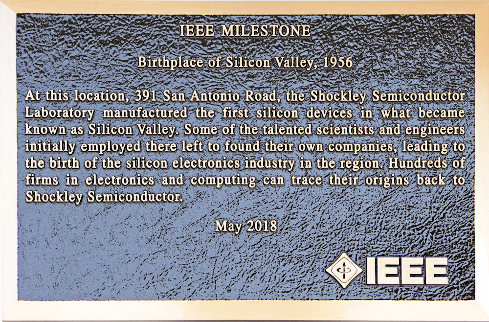
IEEE Milestone plaque commemorating the founding of Shockley Semiconductor Lab in 1956.
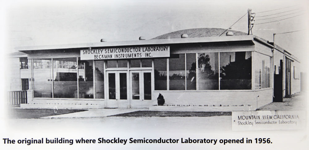
Shockley Semiconductor Laboratory set up shop in a rented, one-room Quonset hut.
The fountain, which is located behind the building facing the street at 391 San Antonio Road, is topped with a gigantic chrome-plated depiction of the silicon crystal lattice. The sculpture strongly reminds me of a similar chrome sculpture (actually, it’s a building) called the Atomium, which is located in Brussels, Belgium. It was built in 1958 for the Brussels World’s Fair. However, the Atomium depicts an iron crystal instead of silicon.
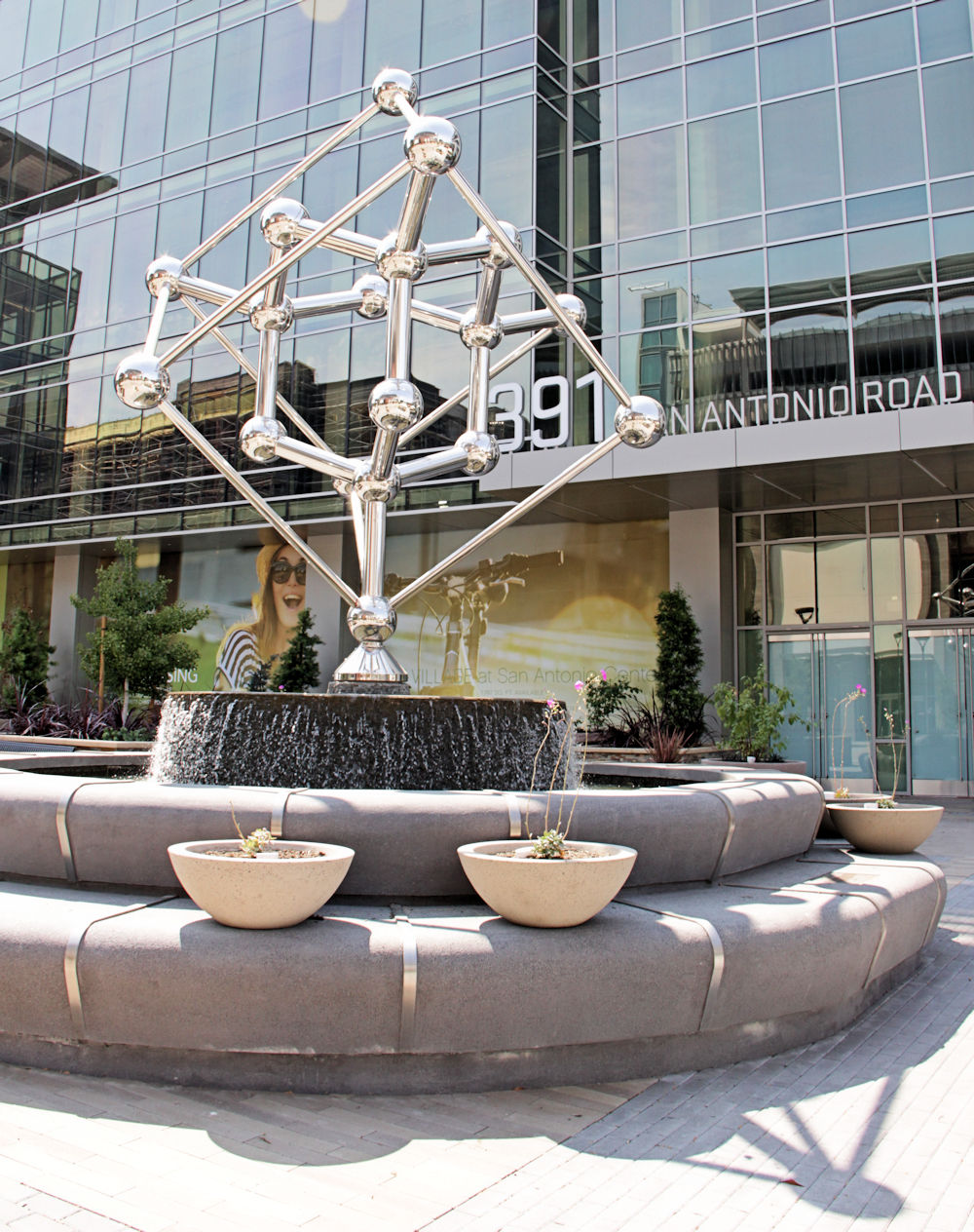
This fountain at 391 San Antonio Road depicts a silicon crystal lattice to commemorate the reason that Shockley Semiconductor Laboratory was founded.
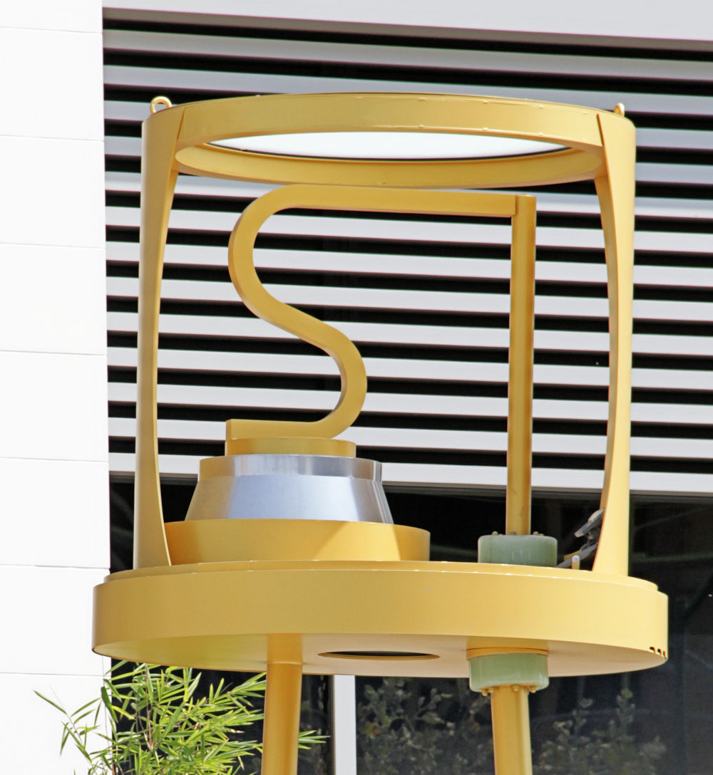
Three Brobdinagian sculptures created by the collaborative artistic team of Mary Bayard White and Vickie Jo Sowell sprout from the sidewalk in front of 391 South San Antonio Road. The sculptures depict early semiconductor devices including a 2N696 transistor and two versions of Shockley’s 4-layer diode. They’re quite detailed, all the way down to the glass insulator on some of the legs of the devices and the schematic diagram of an oscillator based on the transistor and Shockley diode that’s etched into the sidewalk. One giant version of the 4-layer Shockley diode is shown fully packaged and wired into the sidewalk circuit. The other diode sculpture is cut away so that you can see how it was constructed. There doesn’t seem to be any explanations for these devices on site but artist and educator Mary White has a page of explanation on her Web site. Shockley Semiconductor didn’t make the 2N696. It was an early NPN silicon transistor manufactured by Fairchild.
![]()
A gigantic 2N696 transistor now stands guard outside of 391 San Antonio Road in Mountain View, CA.
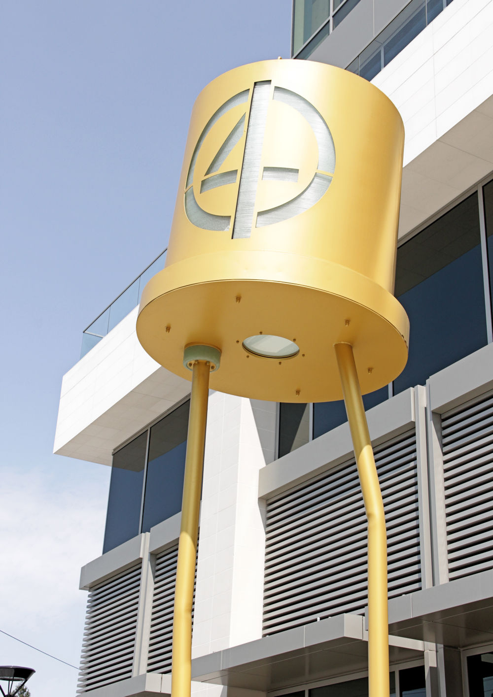
Shockley’s 4-layer diode, writ large.
Cutaway version of Shockley’s 4-layer diode.
All photos taken and edited by Steven Leibson.


One thought on “391 San Antonio Road: The House that William Shockley Built (and Destroyed)”