

I’m happy (albeit puzzled) to tell you that things seem to be getting better with respect to verifying FPGA, ASIC, and system-on-chip (SoC) designs. The reason I say this is that the last time I turned my attention to this arena, people were saying that the design and verification phases of a complex device consumed 30% and 70% of the total development time, respectively. By comparison, someone recently informed me that these numbers are now more like 50% and 50%, which means either we’ve become better at doing verification or worse at doing design.
As you may recall, about six weeks ago as I pen these words, I gave the keynote presentation at the FPGA Forum in Norway (see Not Much Happened, or Did It? and All Change! and When Supercomputers Meet Beer Pong). While I was there, I attended a salmagundi of other presentations, one of which was given by my old chum Espen Tallaksen, who is CEO, Co-founder, and Director of FPGA and Space Technology at EmLogic (which, if you happened to be wondering, stands for “Embedded Logic”)
EmLogic is an independent design center for embedded systems in general and FPGAs in particular. Although EmLogic is a relatively new arrival, having been formed on 1 January 2021, it’s already become established as the leading FPGA design center in Norway and Scandinavia. EmLogic has also established itself as a leading training provider with respect to FPGA design and verification, running courses around the globe in public classrooms, on-site, or online.
In addition to design consulting and services, EmLogic is also a verification IP and methodology provider in the form of UVVM (Universal VHDL Verification Methodology), which is an open-source library and methodology for verifying FPGAs and ASICs/SoCs that is available from GitHub. Furthermore, in addition to being the initiator and chairperson for the FPGA Forum, Espen is also the initial author and architect of UVVM.
When Espen started his presentation, he opened up with a slide containing a few quotes, including “Software designers look at other code with horror” and “RTL sets new standards of awfulness” and “The majority of designs are almost unintelligible to another designer.” I must admit that I agreed with all of these quotes, which was fortuitous, because it turned out that Espen was quoting me from my book The Design Warrior’s Guide to FPGAs.
Espen says that it’s obvious that we have to do lots of verification, but that we can be far more efficient when it comes to creating the verification suite, defining testbenches, and debugging the design.
As an aside, one thing that threw me when I first met Espen at the first FPGA Forum I attended back in 2012 was that he has a Scottish accent. I was reminded of this on my recent visit. At first, I thought this might just be the way Norwegians sound when they are speaking English. However, it turns out that Espen studied at the University of Glasgow, so that’s one less thing for me to worry about, but we digress…
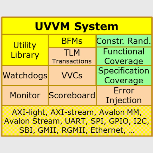
When it comes to verifying your FPGA or ASIC/SoC design, you will have some sort of verification infrastructure around the design-under-test (DUT)—something that writes data into the DUT, something that reads responses from the DUT, and something that controls the different tests and reports any results. The key aspects that you want from your verification environment and solution are Readability, Understandability, Modifiability, Maintainability, Extensibility, Debuggability, and Reusability.
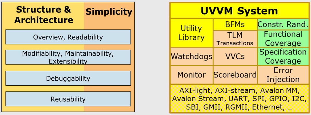
UVVM enables quality and efficiency (Source: EmLogic)
I have to admit that the verification of today’s uber-complex FPGA and ASIC/SoC designs is not my area of expertise, but I’ll try to convey a hint of a sniff of a whiff as to what this is all about. We’ll start with the base/entry level in the form of the Utility Library.
Suppose the design includes a simple interrupt controller (IRQC) module as shown below. Let’s assume that this controller has a clock input, an asynchronous reset, a simple bus interface (SBI) for the external CPU to reach its internal registers, ‘n’ different interrupt sources, and the resulting interrupt going to the CPU.
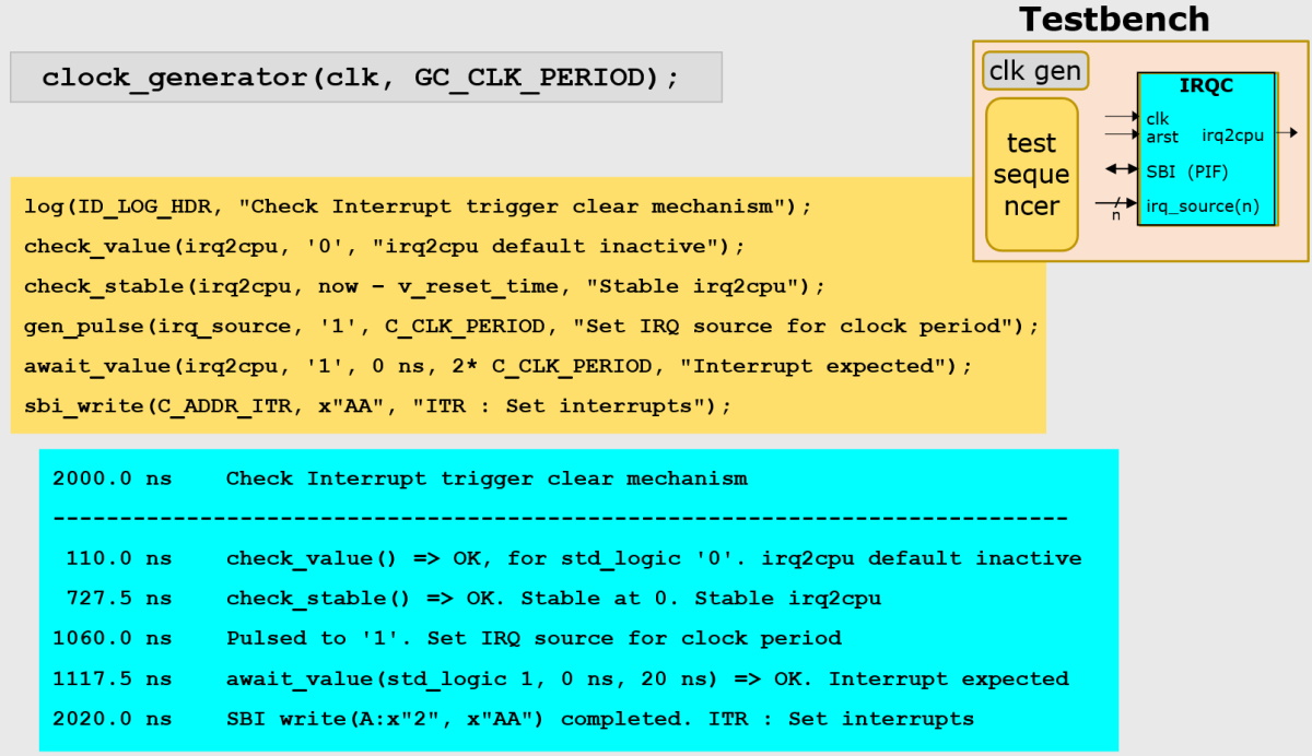
Example of test sequencer code and transcript log (Source: EmLogic)
The UVVM Utility Library contains a bunch of functions and procedures that can be used to build a testbench to exercise this IRQC module. We start with a clock generator, which can be instantiated by calling a procedure from the Utility Library (the statement in the gray box). Next, we create the test sequencer, which consists of a set of procedure calls (the statements in the orange box). When the test sequence is run, the results are shown in the transcript log (the blue box). (Note that this is a simplified transcript—it’s also possible to set/display prefixes, message IDs, and scope.)
Being able to build a testbench using these predefined functions and procedures greatly simplifies the work for whomever has designed the IRQC module and allows them to verify the module much, much faster than if they had to create the test functions and procedures themselves.
Remember that this is just an example of the entry level to UVVM. Next, we have a cornucopia of bus functional models (BFMs) accompanied by a plethora of supported interfaces (AXI-light, AXI-stream, Avalon MM, Avalon Stream, UART, SPI, GPIO, I2C, SBI, GMII, RGMII, Ethernet…). These are also open source and free.
In addition to evaluating functional coverage and specification coverage, UVVM also boasts sophisticated constrained random capabilities, including the ability to add weights to the random values.
I fear we’ve only scratched the surface of this topic, but we’ve reached the boundary at which I can talk knowledgeably. Suffice it to say that you can also set things up to check the DUT for simultaneous activity, which means the system can start transactions on multiple interfaces at the same time (or skew them as required) to root out any problematic corner cases.
Espen started work on UVVM about 15 or 16 years ago. It was first released as open source in 2015, since which time its usage has grown in leaps and bounds.
Mentor Graphics (now Siemens EDA) uses a company called Wilson Research to perform a survey once every two years on ASIC/SoC and FPGA development. The folks at Wilson Research look at lots of different aspects, like how many people are using the various languages and the categories of bugs they are finding. One of the things they look at is how many people are using the various verification systems. In the 2020 survey, UVVM came out on top for VHDL verification methodologies.
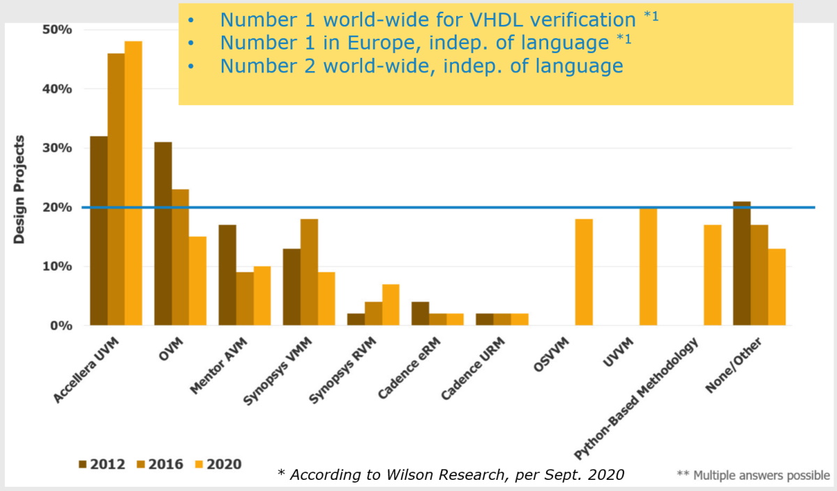
FPGA verification methodologies, world-wide, all languages (Source: EmLogic)
The results from the 2020 survey show that UVVM is the #1 world-wide for VHDL verification. Espen joked that, almost 20 years ago, someone told him that VHDL was dying, and he should start using SystemC. Today, according to Wilson Research, VHDL is used by more than 50% of designers world-wide. Espen says that this number is between 80% and 90% in Europe. Even in the USA, which is a bastion for Verilog and SystemVerilog, VHDL is commonly used in military and space projects. Furthermore, UVVM is the fastest-growing verification methodology independent of language, with its usage exploding by 100% in the two years between the 2018 and 2020 surveys.
One of my heroes in verification space (where no one can hear you scream) is Brian Bailey. I don’t think it’s hyperbole to say that Brian is one of the foremost verification authorities in the world. In fact, I attended a training course on SCAN design that was presented by Brian almost 40 years ago (where does the time go?). I haven’t had a chance to talk to Brian about UVVM yet (I’m sure he knows all about it), but I will be doing so at the earliest opportunity. In the meantime, I’d love to hear your thoughts on all of this.


Hi Max,
It would be interesting to revisit this article using the updated numbers from the 2022 Wilson Verification Survey (released in November). See: https://blogs.sw.siemens.com/verificationhorizons/2022/11/21/part-6-the-2022-wilson-research-group-functional-verification-study/
There you can see that FPGA is dominated by VHDL. You can also see that the survey has lots of variation through the years.
Maybe you would like to do an article on OSVVM.
Cheers,
Jim
Hi Jim — I’m up to my armpits in alligators at the moment but all things are possible for the future — I’ll also ask Espen if he would care to comment here
Hi Max,
Yes, Jim is correct. VHDL is in fact used in more than 50% of all FPGA projects, and the survey clearly shows that VHDL is also the leading HDL for FPGA verification.
I would assume that verification methodologies/libraries like UVVM and OSVVM are contributing to the strong position of VHDL.
– Espen
Hi Max,
> I’m up to my armpits in alligators
I suppose that is better than being up to your eyeballs. 🙂
If you have enough time to click the link you will see that in 2022, OSVVM regained the title of worlds #1 VHDL verification methodology.
Cheers,
Jim