


Last December, Lattice Semiconductor announced the Avant-E family of mid-range FPGAs (see “Lattice Strides Into the Mid-Range FPGA Arena With Avant”), and, at its Developer Conference this month, the company announced an expansion of the Avant family tree through new Avant-G and Avant-X FPGA families. The Lattice Avant-G family is designated as the general-purpose, mid-range FPGA family, and the Avant-X FPGAs are designed specifically for networking applications. Lattice defines “mid-range” as FPGAs that incorporate 100K to 500K logic elements. This definition seems to fit well with other FPGA vendors’ offerings, including the Intel Agilex 5 families (50K to 656K logic elements) and the AMD/Xilinx Artix Ultrascale+ (82 to 308 logic cells) and Spartan UltraScale+ FPGA families. (See “Intel Introduces Two Monolithic Agilex FPGA and SoC Families, Part 2: Sundance Mesa is now the Agilex 5 E-Series” and “Arrow reveals first Dev Board for Intel Agilex 5 FPGAs, with two more boards planned.”)
Like the previously announced Avant-G FPGAs, the Lattice Avant-G and Avant-X FPGAs are built with TSMC’s 16nm FinFET process technology. The programmable logic fabric implemented in these three Avant FPGA families appear to be identical. The difference between these two new FPGA families is really in the peripheral blocks that Lattice has placed around the programmable logic in these devices. All three of the Avant FPGA families are based on TSMC’s 16nm FinFET process technology, and Lattice claims that this more advanced process technology doubles the performance of its FPGAs while significantly lowering power consumption. With the new process node, Lattice also gets smaller die size from TSMC’s 16nm process, which the company has capitalized upon by offering smaller device packaging.
Initially, the company will be offering three devices in each of the Avant-G and Avant-X device families. The Avant-G30, -G50, and -G70 FPGAs incorporate 262K, 409K, and 637K “system logic cells” (SLCs); 14.4, 22.7, and 35.6 Mbits of on-chip block RAM; and 700, 1120, and 1800 DSP blocks, each with 18×18-bit fracturable multipliers, respectively. These FPGA fabric resource quantities are the same for the Avant-X30, -X50, and -X70 FPGAs as well. Both new Avant FPGA families also have memory controllers that support DDR4 and LPDDR4 SDRAMs operating as fast as 2400 Mtransfers/sec. The Avant-X FPGA memory controller also supports DDR5 SDRAMs operating at 2100 Mtransfers/sec.
The differences between these two families mostly lie in the on-chip peripherals. Both the Avant-G and -X FPGAs incorporate 12 to 28 high-speed SerDes ports, depending on the device selected. The Avant-G SerDes ports can operate as fast as 12.5 Gbps, and the Avant-X FPGA ports can operate as fast as 25Gbps. The general-purpose Avant-G FPGAs can support a PCIe Gen3 x8 port with a hardened link layer, and, thanks to the faster SerDes ports, the Avant-X devices can support a PCIe Gen4 x8 port, also with a hardened link layer. Both new FPGA families also support the MIPI D-PHY interface at a maximum data rate of 1.8 Gbps.
Lattice disclosed these features 12 months ago during the initial Avant FPGA launch and is now delivering on its promises with the two new FPGA families. Early access customers have had samples of these new Avant FPGAs since Q2 of 2022, and the company is now ready for general sampling. Development boards are also said to be available.
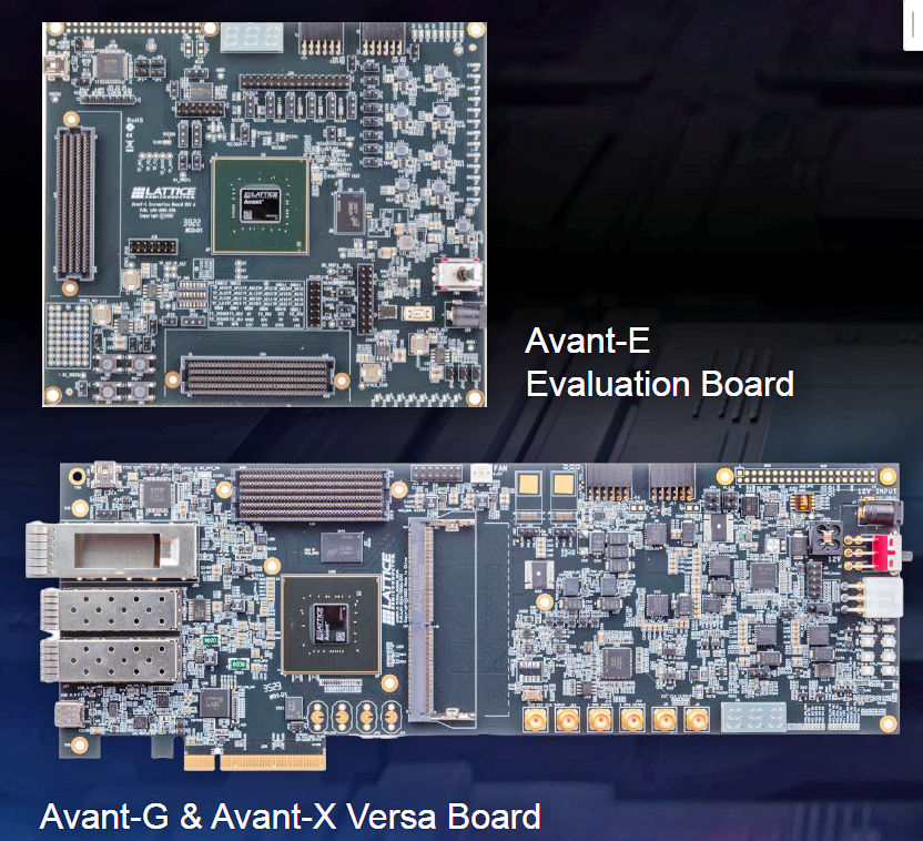
Lattice has evaluation and development boards ready for the new Avant-G and Avant-X FPGAs. Image credit: Lattice Semiconductor
Lattice has focused on reducing the pcb footprint of these FPGAs and offers small-form-factor, fine-pitch packaging options. The smallest member of each of the two new FPGA families fits in an 11x9mm package while the largest of the three FPGAs in each family fits in a 15x13mm package. The middle member of each FPGA family fits in a 12x12mm package. Larger package options are also available if fine-pitch pcbs are not to your liking.
Lattice made it clear that these devices compete in the mid-range FPGA segment by offering comparisons with Intel Arria 10 and Arria V GZ and AMD/Xilinx Kintex 7 and Kintex UltraScale+ FPGAs. It would be most embarrassing if Lattice’s brand spanking new FPGAs compared unfavorably with these older FPGAs. Altera announced what is now called the Intel Arria 10 FPGAs back in 2013. That’s ten years ago. Those FPGAs are based on TSMC’s 20nm planar FET process. The Arria V GZ devices, based on TSMC’s 28nm planar FET process technology, are a year older than the Arria 10 FPGAs. Xilinx introduced the Kintex 7 FPGAs, which are based on TSMC’s even older 28nm planar FET process, back in 2012. The AMD/Xilinx Kintex UltraScale+ devices, based on TSMC’s 16nm FinFET process, were first discussed in 2015. So, the way to interpret this announcement from Lattice is that the company is now ready to compete in the mid-range FPGA market with a broad silicon portfolio that’s as fast or faster than the existing FPGAs in this segment, while delivering better power consumption.
However, it takes more than silicon to compete in the FPGA arena. Software is an essential part of the winning strategy. In fact, FPGA vendors have long known that the design software bundled with their FPGAs strongly contributes to the “stickiness” of their silicon and helps ensure that a customer, once captured, stays with the same FPGA vendor for many years because the pain of learning another vendor’s design tools is just too great.
Consequently, Lattice has been preparing its software arsenal for the company’s expanded foray into the mid-range FPGA markets. Lattice Radiant, the company’s foundational FPGA development tool, has been augmented with capabilities specific to the Avant-G and Avant-X FPGA families, as has Lattice Propel, which allows designers to create FPGA-based processor systems. Lattice also offers a slate of solution stacks, including Lattice Automate, for industrial automation applications; Lattice mVision, for embedded vision system designs; Lattice sensAI, for FPGA-based Machine Learning applications; and Lattice Sentry, for developing FPGA-based Platform Firmware Resiliency (PFR) Roots of Trust. If you’re developing Open Radio Area Networks (ORANs), there’s a Lattice solution stack for that too. Mirametrix’s Glance software – which enables the development of face-recognition and eye-tracking applications – is also available and makes use of the Lattice sensAI solution stack.
One thing that remains as a glaring omission in Lattice’s mid-range Avant FPGA offerings is a hardened processor core. The company continues to rely on soft microprocessor cores, which are at an inherent disadvantage to hardened processor cores with respect to speed, power, and silicon consumption. It’s not as though it’s difficult to put a hardened processor subsystem on an FPGA. Intel and AMD have been doing it for years with their SoC FPGA and Zync products. However, Lattice doesn’t seem to perceive a need for hardened processor cores on its FPGAs, so if you want a processor in your Lattice-based FPGA system (and who doesn’t?), then you’ll either add one as a separate chip or spend some logic cells to instantiate a processor and its support logic in the FPGA’s programmable logic fabric. That’s a colossal waste of logic cells, in my opinion. It makes more sense to use hardened processors if a standard core will suffice, and they usually will in FPGA-based systems.
Whether these offerings will allow Lattice to further drill into the mid-range FPGA arena is anyone’s guess. Certainly, existing Lattice customers will be thrilled to have more choices from Lattice. However, there’s a large barrier when trying to lure customers from Intel’s or AMD/Xilinx’s mid-range FPGA territory. Do the Avant FPGA families offer sufficient incentive to switch? We’ll need to wait a bit to see.


