


Lattice Semiconductor is moving upscale with its new mid-range Avant FPGA platform. After spending the last several years taking low-end market share from its bigger FPGA competitors, essentially while they weren’t looking, Lattice has decided that a similar opportunity awaits in mid-range programmable-logic parts. I think the jury is out there. We’ll need to wait to see if Lattice’s perception is correct. Meanwhile, system designers can welcome a new player in the mid-range market, which Lattice is defining as FPGAs with as many as 100K to 500K logic elements. According to Lattice, programmable-logic devices based on the mid-range Avant FPGA platform will compete directly against Intel Arria and AMD/Xilinx Kintex mid-range FPGAs.
Understand that Lattice plans to use its new Avant platform, which is based on TSMC’s 16nm FinFET process technology, to generate several mid-range FPGA families. Lattice’s Nexus platform, which the company introduced three years ago, is based on Samsung’s 28nm FD-SOI process. You can expect that the FPGAs developed using the Avant platform will be faster, have higher capacity, and will sport more features than FPGAs based on the company’s earlier Nexus platform.
Here are a few of the salient features that Lattice announced for the mid-range Avant FPGA platform:
- As many as 500K programmable logic elements, based on 4-input LUTs. That’s 5x more logic cell capacity than was possible with the company’s Nexus earlier platform.
- 18×18-bit, DSP blocks, fracturable into two or four smaller units
- 25 Gbps SerDes ports
- Hardened PCIe Gen4 x8 support
- Built-in support for SDRAMs with a hardened DDR memory interfaces including DDR4 and DDR5
- Hardened, post-quantum cryptographic security engine
Lattice has provided some performance numbers relative to the competition; however, the company chose to compare its new mid-range Avant FPGAs with members of the Intel Arria V and AMD/Xilinx Kintex-7 FPGAs. Of course, since this is Lattice’s announcement, Avant is faster and consumes less power than those competing devices, which are indeed mid-range devices in terms of logic cell capacity. However, Altera and Xilinx announced their Arria V and Kintex-7 FPGA families in 2011 – more than a decade ago – so you sort of know which parts are going to win in these comparisons even before you see the numbers. It would be much better, much more informative, and more appropriate to see the Avant FPGAs benchmarked against newer versions of AMD/Xilinx’s and Intel’s competing mid-range FPGAs such as the Arria 10, Artix UltraScale+, and Kintex UltraScale+ FPGAs.
It’s important to understand that Lattice’s Avant is an FPGA platform, not a product family, in the same way that Lattice’s Nexus platform isn’t an FPGA family. Lattice’s FPGA families based on its Nexus platform include the Certus-NX, CertusPro-NX, CrossLink-NX, Mach-NX, and MachXO5-NX FPGA families. The Certus-NX and CertusPro-NX families have maximum logic cell counts of 39K and 100K respectively and are general-purpose FPGAs. The CrossLink-NX family is specifically adapted for video applications and incorporates video-centric interfaces such as MIPI D-PHY. The Mach-NX and MachXO5-NX families have smaller logic cell counts of 8.4K and 25K, respectively, and they incorporate on-chip flash memory for storing the FPGAs’ configuration data. For many low-end applications, eliminating the Flash memory configuration chip is a real advantage, so these Mach devices have a nice little design niche.
Lattice Semiconductor plans to create the same sort of family proliferation from the Avant platform, and the company announced the first Avant-based FPGA family, the Avant-E FPGA family, along with the platform. The announcement included three members of the Avant-E FPGA family: the 200E, the 300E, and the 500E with 196K, 306K, and 477K logic elements, respectively. These devices incorporate 700, 1120, and 1800 DSP blocks, respectively, in addition to the logic cells. Like the company’s CrossLink-NX family, the Avant-E FPGA family supports the MIPI D-PHY interface, but none of the Avant-E FPGAs have high-speed SerDes transceivers. These three Avant-E family members have as much as 36 Mbits of on-chip SRAM and support external DDR4 and LPDDR4 SDRAM with integrated memory controllers.
Lattice’s market research into mid-range FPGAs uncovered a need for small-footprint devices, so the Avant-E 200E FPGA is available in an 11mm x 9mm, small-form-factor package. The larger members of the Avant-E FPGA family are available in 12mm x 12mm and 15mm x 13mm packages. Larger packages with more I/O pins are also offered. Lattice is already manufacturing the largest member of the Avant-E FPGA family, the 500E, and has been providing these devices on evaluation boards for early-access customers for several months. The evaluation board is now broadly available. Here’s a photo of that board:
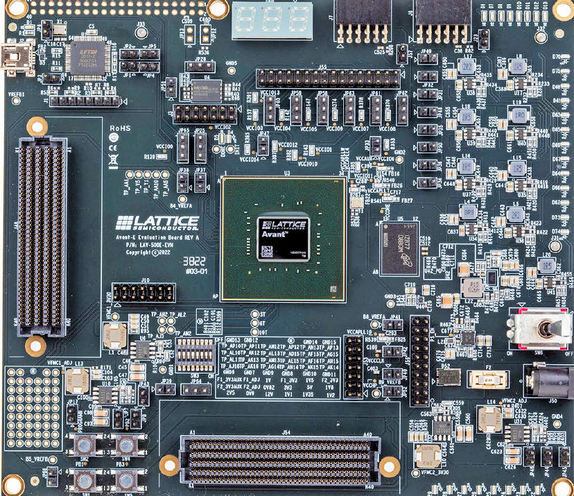
Avant-E FPGA Evaluation Board
It’s no longer possible to simply release parts into the FPGA market and expect them to win sockets. The winning combination now requires development tool support, a broad IP library, reference designs, and software stacks. Lattice has already upgraded its Propel design environment and existing development tools to support the Avant-E FPGA family. Existing Lattice customers should therefore find the development tools for devices based on the Avant platform to be very familiar.
Because the Avant-E FPGAs now have five times the number of available logic elements to work with, large IP blocks become all that much more important. The company says it has signed a long and growing list of IP suppliers to support its Avant-E FPGAs.
One thing seems glaringly absent in the Avant-E FPGA family. None of these devices incorporate a hardened microprocessor subsystem. Both Intel and AMD/Xilinx have offered FPGAs with hardened microprocessor subsystems for a decade, for one simple reason: to a first-order approximation, 100 percent of all systems based on FPGAs also incorporate one or more microprocessors. If the FPGA does not incorporate a microprocessor, then it must be added externally. In the past, the microprocessor cores of choice have all been based on Arm cores, with the exception of the PowerPC processor on Xilinx’s ill-fated Virtex-II Pro family, but these days, cores based on the RISC-V ISA also look like a very good choice because of that ISA’s global momentum and community support.
I specifically asked Lattice about the absence of a processor core in the list of planned features for FPGAs based on the Avant platform. The company’s response was that customers can use some of the logic cells in the FPGA fabric to add a microprocessor core of their choosing. Of course, that is a true statement. Lattice has two RISC-V processor cores in its IP library. Although both Intel and AMD/Xilinx offer hardened microprocessor subsystems on many of their devices, both companies continue to offer soft-core RISC processor IP – Nios and MicroBlaze respectively – and many designs do employ these soft cores. Intel recently added the Nios-V soft core to its IP library, which is based on the RISC-V ISA.
So technically, Lattice is correct. Customers that want a processor on their FPGA can add one using a soft core. However, doing so is a colossal waste of logic cells, in my opinion. A soft processor core consumes a lot more silicon and runs much slower than a hardened microprocessor core on the same FPGA. If using a microprocessor or two were a rarity for FPGA-based systems, Lattice’s stance would make sense to me. Offering a pair of hardened, on-chip microprocessor cores that can operate in lockstep for high-reliability and safety-related applications makes more sense to me. However, it’s the market that will ultimately deliver judgment on this facet of Lattice’s Avant platform, not my opinion.
Certainly, this omission is not a fatal step on Lattice’s part. Nothing prevents the company from adding a future family of Avant-based FPGAs with hardened processor cores. The slide deck that the company distributed with its announcement indicates plans to introduce two more Avant-based FPGA families in 2023 and several more families in subsequent years. If the demand is there, and I expect that it is, I am certain that Lattice will be adding hardened processor cores to at least one future Avant FPGA family. Avant-P, perhaps?
In addition, Lattice has developed several major application-specific software stacks and solutions for its prior FPGA families, which the company is extending to FPGA families based on the Avant platform. These software offerings include:
- Lattice SensAI for FPGA-based Machine Learning and Artificial Intelligence applications
- Lattice Sentry for developing NIST SP800-193-compliant, FPGA-based Platform Firmware Resiliency (PFR) Roots of Trust
- Lattice mVision for embedded vision applications including machine vision, robotics, ADAS, video surveillance, and drones
- Lattice Automate for industrial automation applications including CNC, robotics, scalable multi-channel motor control with predictive maintenance, real-time industrial networking, and local-to-cloud networking
- Lattice ORAN for 5G-ORAN application acceleration using FPGAs
It’s great to welcome another worthy gladiator to the mid-range FPGA arena. Today’s mid-range FPGAs are more capable than high-end devices from two decades past. It’s a hotly contested arena because of the advantageous price and performance of competing devices. Competition hones the skills of all players and Lattice’s entry into this arena with the mid-range Avant platform is sure to capture the attention of prospective customers. It’s also certain to get Intel’s and AMD/Xilinx’s attention. Let the games begin.


Yeah, sure, RISCV is the future! Hooey!! Soft core CPU? Phooey!
Like it or not Load/Store and off chip memory will never have good enough performance DDR4, DDR5, DDR/Infinity, or whatever.
So these guys left the door open for something new……….. What if the design tools and design approach were based on design rather than Synthesis? Since day one, or maybe day 2 it has been a dream that programmers could design logic. Well 50 or so years later we have HDL, System Verilog, VHDL, and SystemC. Let’s throw in RISC(V) and all the other children!
Well, C# has recently added conditional assignment so there is a complete design, debug, API, IDE, AST, and SyntaxWalker all open source just waiting for this opportunity.
See you later…………
Feel free to scoff all you like, Karl. Sometimes, you just need a processor. I’m a hardware designer myself, but I’m not designing hardware to run a GUI or an Ethernet protocol stack. Those tasks are already done, debugged, and canned. It’s simply more efficient to run those sorts of things on a microprocessor core or chip. Arm has thousands of customers, especially when you consider the number of people using Arm-based microcontrollers, and RISC-V International has more than 3000 members to date. Sure, these people could all be delusional, but they also constitute an attractive market with solid commercial potential. After 50 years of commercial success, I surely do think these microprocessors might just catch on. However, just to be clear, no one says you must use a processor.
> Since day one, or maybe day 2 it has been a dream that programmers could design logic. Well 50 or so years later we have HDL, System Verilog, VHDL, and SystemC. Let’s throw in RISC(V) and all the other children!
Yeah. LEave it to a programmer to make physical things. VHDL and Verilog – what a “great” tools. First you bullshit someopne to write basically a code to describe a circuit and then you have to have multiple laqyers of tools to de-bullshit that back into something that could work ( or not) in reality.
You’ve been trying too hard to lick Lattice guys arsehole by avoiding questions like these:
* They like to talk about IoT and edge applications a lot, but when are we to see an actual Lattice FPGA, that can do PCIe4 ?
* When are we to see partial self-reconfigurability while running, like Xilinx can do with their ICAP mechanism. At the lower and middle end one has to be able to use whatever asset one can and this would be great – FPGAs are bloated by their nature. WHy can’t one use re/configuration logic for something useful at “runtime” ?
* What happened to their commitment to open source ? When are they to seriously open documentation to Yosys and similar projects
* Why do they have so fascistic pricing policies and so closed free options for IDE ? How many can pay $2k+ per year for a licence just so that they can configure effing thing ?
* If I’m not mistaken, some of that Avant architecture is to trickle-down into MachXo(5?) series. Are we ever to see actually useful onboard user FLASH in these things ? Something with 32 bus, that could be used for a code of softCPU etc ?
* Most of the cool stuff of the new series is yet to come in 2023 and 2024. Well, competiton is working big time. How cool will this still be in 20 year time ?
Oh, one more question from me:
If the Lattice went for pure FPGA approach (no hardCPU), why aren’t there more optimizations toward making more efficient soft-CPU implementations ? Why is octa-SPI an option that we are yet to see sometime in the future ? It would be a great option for such core – a FLASH with dual use: both fast configuratin and efficient boot code execution of the softCPU.
IT would also be nice to see some logic block that could be used for implementation of soft-CPU or similar state machines ( implementation of register set, ALU pathways etc).
As far as I can see, Avant is just Certus, tweaked for newer process nodes etc.
Well Mr. Brane, if an article containing criticism of Lattice is licking the company’s butt, then yep, guilty as charged. All your brave and valid questions really ought to be directed at Lattice, not to an article in an online publication. We report the news, not make it. It may shock you to know that Lattice doesn’t ask me for advice on future products. I only get to report on what they’ve done, which I try to do as factually as possible. You obviously need some real features for your application for which Lattice’s products fall short.
As for your final question as to why there aren’t more optimized soft CPUs for FPGA use, the answer is that the FPGA companies would love to accommodate you. One problem: there aren’t such things. FPGA implementations of any IP core are roughly 10x off in all three critical dimensions (power, performance, area) relative to standard-cell ASICs given the same process technology. That’s especially true for RISC processors, where their large multi-port register files get really tangled and congested and are hard to route in any sort of compact form.
In exchange for those disadvantages, FPGAs give you field programmability. For standard IP cores like CPUs, where you want to run a standard ISA, field programmability gives you very few advantages, except that you’re not locked into one CPU architecture. Want some flavor of Arm? Great. Want RISC-V? Great. Want a LEON (a SPARC processor for space applications)? Great. Want them all on one device? Sure, why not? If you really want a fast CPU with ASIC-like speeds, then a hard core is indeed what you want.
>We report the news, not make it.
Your article was clearly more than just “reporting the news”. If you are to add your own remarks, you might as well ask valid questions.
>As for your final question as to why there aren’t more optimized soft CPUs for FPGA use, the answer is that the FPGA companies would love to accommodate you.
That wasn’t my question. I was asking, since they opted to go for pure FPGA, why haven’t they optimized some part of FPGA switch matrix to be able to efficiently implement soft-CPU or similar complex state machine.
>FPGA implementations of any IP core are roughly 10x off in all three critical dimensions (power, performance, area) relative to standard-cell ASICs given the same process technology.
I know that, hence my question – FPGA is “high bloat” by definition. Much of that is in switch matrix. So, why haven’t they done some optimizations, perhaps even special hardened block that would ease u and speed up such “semi-soft” implementation.
The special optimization you are looking for, Mr. Brane, is called a hardened microprocessor core. They’re pretty small when hardened and they work really well. You should try one.
>The special optimization you are looking for, Mr. Brane, is called a hardened microprocessor core. They’re pretty small when hardened and they work really well. You should try one.
Nope. No use of searching for hardened CPU sore in the FPGA that has none, as a I said. I was looking for specialized connective structure and hardened “macros” that could be connected into one with much less overhead than classic FPGA elements would bring. This would bring to the table something that I could see as a significant innovation that the Lattice claims for the new Avant series…