

Early microprocessors straddled two major computing epochs. During the first epoch, stretching from the late 1960s through the 1970s, computer system engineers designed and implemented minicomputer processor architectures and processor boards using TTL parts, bipolar PROMs, stone knives, and bearskins. Each minicomputer maker – including Digital Equipment Corp (DEC), Data General (DG), Prime, Computer Automation, IBM, Burroughs, HP, Four-Phase, NCR, and Univac – had their own, proprietary minicomputer architectures, ISAs, and dedicated peripherals. It was the wild, wild West. During the second epoch, which partially overlapped the first epoch, some computer manufacturers and some semiconductor vendors started designing LSI chips with increasingly large processor chunks integrated onto an IC, culminating in the development of single-chip microprocessors.
The first commercially successful, single-chip microprocessor – an early child of the second epoch – was the 4-bit Intel 4004, which just celebrated its 50th birthday on November 15, 2021. (See “Say Happy 50th Birthday to the Microprocessor, Part I” and “Say Happy 50th Birthday to the Microprocessor, Part 2.”) The 4004 microprocessor arrived with much hoopla, but Intel had a second microprocessor in development at the same time. That microprocessor was the 8-bit Intel 8008. The stories of these two processors intertwine in many ways, and they’re independent in others.
Like the Intel 4004 microprocessor, an external customer drove the development of the Intel 8008 microprocessor. For the Intel 4004 microprocessor, the external customer was Busicom, a Japanese calculator company that wanted the Intel 4004 to build high-end desk calculators. Intel designed and built the 4004 and three companion chips for Busicom and then later negotiated the right to market the Intel 4004 microprocessor to other companies, in exchange for price concessions made to Busicom on the parts. Intel introduced the 4004 microprocessor to the world on November 15, 1971.
The 4-bit Intel 4004 microprocessor was part of a 4-chip set, including the microprocessor, a ROM, a RAM, and a shift register for I/O expansion. This 4-chip set, dubbed the Intel MCS-4, represented a walled garden. The microprocessor’s unique, multiplexed, 4-bit bus formed the garden wall. If another chip wanted to communicate with the Intel 4004 microprocessor, it had to implement the control and timing logic needed to interface with that multiplexed bus.
At the time, Intel’s primary business was selling memory, specifically RAMs and ROMs. These memories all had parallel address and data buses. None were directly compatible with the Intel 4004’s unique bus. That was not the vision for the Intel 8008 microprocessor, which was developed with a simpler system bus in mind. The 8008 was designed to use standard RAMs and ROMs, which Intel was making as well.
The external customer for the Intel 8008 was the Computer Terminal Corp (CTC), located in San Antonio, Texas. CTC made an outsized contribution to the Intel 8008 microprocessor’s architecture and ISA. The microprocessor’s definition was based on CTC’s existing plans for an 8-bit, board-level processor built with about 100 SSI and MSI TTL chips. Using their experience with the 4004’s development, Ted Hoff and Stan Mazor at Intel reviewed and tweaked CTC’s planned processor architecture slightly to improve it, to ease its manufacture as a single chip, and to allow Intel to cram the microprocessor into an itty-bitty 18-pin DIP. The architectural tweaks involved changes to the ISA.
CTC made dumb terminals, and Intel was supplying a custom, 512-bit recirculating shift register for that application. CTC wanted to expand into the growing minicomputer terminal business, and it was developing an 8-bit embedded processor board as the foundation for an intelligent terminal that it planned to make. As part of that development, CTC’s Technical Director, Victor Poor, investigated Intel’s 64-bit (NOT Kbit or Mbit) bipolar SRAM as a possible way to implement the CTC processor’s registers. He asked Intel if it could make a custom version of the SRAM by adding a counter to the RAM design, enabling its use as a pushdown stack register.
Intel’s Stan Mazor, who’d worked on the early definition of the Intel 4004, discussed the requirements with Poor, developed a deeper understanding of the CTC processor architecture, and then wrote three proposals for custom chips. Mazor’s first proposal was for an 8-bit register set with a stack counter, per Poor’s initial request. The second proposed chip was a register stack with an added arithmetic unit (conceptually similar to the Four-Phase AL1). The third proposal was for an entire 8-bit CTC CPU on one chip. That one got Poor’s attention.
Mazor didn’t even have a detailed description of the CTC processor architecture or its ISA when he created this proposal, but Poor was sufficiently intrigued by the third proposal to send Mazor the programming manual for the processor, which described the architecture at the assembly-language level. Mazor and Ted Hoff, freshly freed from the Intel 4004 project (and leaving Federico Faggin to develop and sweat over the silicon-gate process and logic implementation details), studied the CTC processor’s programming manual in depth and created a more detailed proposal for a single-chip version of CTC’s 8-bit CPU processor. The Intel salesperson for CTC then got involved, and CTC cut a $3 million purchase order for the one-chip processor on March 18, 1970 for 100,000 parts at $30 apiece. (To see an image of this purchase order, check out Lamont Woods’s article titled “Digital World’s Birth Certificate Written in San Antonio.”)
Freshly hired Hal Feeney became the chip designer for the 8-bit processor project. Mazor and Feeney started their development with the proposal Intel provided to CTC. However, the project quickly went on hiatus because there was some question as to whether CTC was really committed to the development of this custom chip. (A pause of similar duration had occurred in the development of the Intel 4004, but there the fault was entirely Intel’s.) With the 8-bit microprocessor project stalled, Feeney went off to help Federico Faggin finish development of the 4004 microprocessor and the MCS-4 chipset.
There is something very interesting about the detailed microprocessor proposal that Intel sent to CTC. The proposal accidentally contained a design flaw that would prevent the microprocessor from properly servicing interrupts. As originally defined, the interrupt mechanism would cause the microprocessor to call the interrupt service routine without first putting the return address onto the processor’s stack, so there was no way for the interrupt service routine to return from the interrupt. This flaw made the proposed interrupt mechanism useless.
Around this time, Texas instruments (TI) also started developing a single-chip processor for CTC, based on CTC’s specification and at CTC’s request. TI’s processor would be called the TMX 1795. Although TI originally proposed a 3-chip set for CTC’s processor, it switched to a single-chip design sometime after Intel made its own proposal to CTC. TI built the TMX 1795 on a very large die, which would not have been economical to produce in volume. In addition, according to Feeney, darned if the TMX 1795 didn’t have an identical interrupt design flaw that worked just the way that Intel had mistakenly defined it.
TI built the TMX 1795 but didn’t succeed in selling it to CTC and never successfully marketed the device. Instead, TI went off and successfully sold tons of TTL, calculator, and other chips. The TMX 1795 microprocessor survives in stories and as a few artifacts, including a 1996 video of the device in operation, at the Computer History Museum in Mountain View, California. (For more details about this little-known TI microprocessor, see Ken Shirriff’s blog titled “The Texas Instruments TMX 1795: the (almost) first, forgotten microprocessor.”)
Meanwhile, the 8008 microprocessor’s 6-month project hiatus actually helped Intel debug and improve the design. First, it provided time to reflect on and refine the 8-bit processor’s architecture. The original CTC instruction set included a branch-on-bit instruction. The Intel design team determined that the instruction wasn’t needed and removed it to simplify the processor’s hardware design. At the same time, the Intel design team determined that the processor would greatly benefit from increment and decrement instructions, so they added these two instructions to the 8008’s ISA. The hiatus also allowed the Intel 8008 design team to catch and fix the flawed interrupt mechanism.
In addition, the hiatus provided time for Intel’s breakthrough 1103 1Kbit DRAM to go into production. That was a significant event for many reasons, but the direct benefit to the 8008 project was the 18-pin DIP that housed the first high-volume DRAM. Because that package was now officially sanctioned by Intel’s production group, the Intel 8008 design team could use it to add two more precious pins to the Intel 8008. Previously, the 8008 design team had been restricted to 16 pins, because that was the package that Intel’s production group had on hand.
According to Feeney, those two extra pins were sorely needed to improve the 8-bit processor. Among the benefits: one of the extra pins was used to bring additional state information out of the microprocessor, which helped to implement the microprocessor’s stack and allowed the interrupt mechanism to work properly.
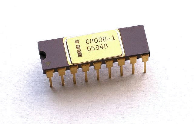
The Intel 8080 Microprocessor was packaged in an 18-pin DIP, which Intel also used for its 1103 1Kbit DRAM. Photo Credit: CPU Collection Konstantin Lanzet
With careful design and Faggin’s semiconductor process and design methodology improvements, some of which he’d developed for Intel’s MCS-4 project, Feeney’s 8008 microprocessor die was only slightly larger than the Intel 4004 microprocessor die, even though the 8008 needed 50 percent more transistors count (3500 transistors versus 2200 for the 4004). Feeney’s design was therefore quite manufacturable. Unfortunately, the Intel 8008 microprocessor, implemented in silicon-gate MOS, ran significantly slower than the bit-serial TTL version of the processor that CTC had designed and implemented. It also required a significant number of support chips to create a complete system, although not as many as the 100 chips on CTC’s processor board, so the savings in chip count when using the 8008 microprocessor weren’t quite as significant as they might have been.
CTC evaluated the Intel 8008 microprocessor in late 1971, and said, “No thanks.” It was too little, too late. The company had already developed its first Datapoint 2200 terminal with the bit-serial TTL processor and was working on an even faster parallel implementation for the next generation of terminals. CTC sold Datapoint 2200 machines until 1979 and upgraded the TTL processor board’s design several times along the way. The TTL processor became faster with each revision.
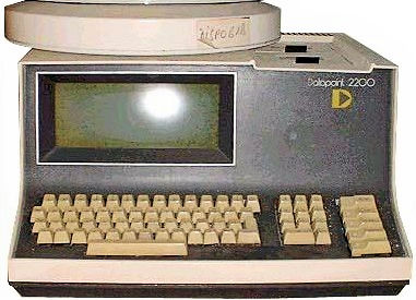
Datapoint 2200 Intelligent Terminal with a removable, 2.5Mbyte hard disk cartridge sitting on top. Photo Credit: www.engcyclopedia.de
The Datapoint 2200 terminal was much more than a terminal. It was a minicomputer that you could program in BASIC or PL/B and was offered with one or two digital cassette tape drives, a companion 2.5Mbyte hard disk drive, and later, with an optional floppy disk drive. Some historians have called it the first personal computer, and it was clearly designed to be a computer, but it wasn’t based on a microprocessor. It merely spawned one. CTC’s Datapoint 2200 intelligent computer/terminal sold so well that the company later changed its name to Datapoint.
Meanwhile, having lost its main customer, Intel now owned the rights to the 8008 microprocessor and decided to sell it commercially. Although many online articles and references use April, 1972 as the introduction date for the Intel 8008, the company announced the microprocessor on March 13, 1972, just four months after announcing the Intel 4004. A few online citations say it was 1974, obviously confusing the Intel 8008 and 8080 microprocessors. However, thanks to Ken Shirriff’s extensive research, the Intel 8008’s formal debut appears to have been a 1-page article, written by Stephen William Fields and titled “8-bit parallel processor offered on a single chip,” which appeared in the March 13, 1972 issue of Electronics magazine (See Note 2 below.)
Intel was now selling not one but two single-chip microprocessors: the 4004 and the 8008. They had a clear lead in this new market.
The Intel 8008 microprocessor has a 16Kbyte address space (using 14-bit addressing, considered immense at the time, and four times larger than the 4004 microprocessor), and a two-phase, 800KHz clock (for the fastest speed grade). According to the data sheet, an 8008 instruction fetch/execute cycle requires a minimum of five processor states, or 10 clocks. That’s a peak instruction execution rate of 80,000 instructions per second.
If measured by today’s microprocessor standards, or even by the standards of 30 years past, Intel’s 8008 is truly feeble and slow. But it was the first commercial, 8-bit, single-chip microprocessor, and you could build useful systems with it. System designers started to incorporate the Intel 8008 into many new products including embedded systems, such as the first two versions of HP’s legendary and long-lived 2640 series smart CRT terminals (take that, CTC!), and several early microcomputers. In addition, the 8008 microprocessor’s introduction helped Intel sell a lot more of its main products, namely DRAMs and EPROMs, by enabling and even encouraging the design of systems that needed semiconductor memory.
The Intel 8080 and 8085, the 8-bit Zilog Z80, and all x86 microprocessors developed over the last half century by Intel and other processor vendors all carry some reptilian DNA from the original Intel 8008. If you don’t believe that, just look closely at the register sets in these microprocessors.
That’s quite a legacy, wouldn’t you agree?
Notes:
- Federico Faggin left Intel and founded Zilog in 1974. He put some 8008 microprocessor DNA into the extremely successful 8-bit Z80 microprocessor, which Zilog announced in 1975. But that’s another story, for another time.
- For an excellent and detailed analysis of the Intel 8008 microprocessor’s design, see Ken Shirriff’s blog titled “Die photos and analysis of the revolutionary 8008 microprocessor, 45 years old.”
- To see the article announcing the 8008 microprocessor in the March 13, 1972 issue of Electronics magazine, see Ken Sirriff’s blog titled “Analyzing the vintage 8008 processor from die photos: its unusual counters,” and scroll down to the “Notes and References” section. There’s an image of the one-page article there. Read the blog along the way, of course, because it’s filled with interesting facts. For example, Shirriff’s reverse engineering shows how and why Intel implemented the 8008 register set using DRAM cells instead of latches (to save transistors).
References:
Oral History Panel on the Development and Promotion of the Intel 8008 Microprocessor, Computer History Museum, September 21, 2006.
Lamont Wood, Datapoint: The Lost Story of the Texans Who Invented the Personal Computer Revolution, Hugo House Publishers, 2012.


One thought on “Happy 50th Birthday to the 8-bit Intel 8008 Microprocessor”