

I think it’s fair to say that the majority of my friends in Embedded Space (where no one can hear you scream) tend to live on the microcontroller (MCU) side of the fence. To put this another way, relatively few of my chums don their “I’m an FPGA Designer” T-Shirts before heading off to work in the morning.
A few years ago as I pen these words, I realized that I was spending an inordinate amount of my time explaining what FPGAs are and how they work their magic to members of the MCU fraternity (whatever they say, I still find it hard to believe their claims that they don’t have special parties and secret handshakes). This prompted me to write a trio, triad, or troika of columns on the topic of FPGAs for MCU Guys and Gals: The Hardware, The Software, and Configuration Techniques and Technologies.
The reason I mention this here is that I just heard from Yoan Dupret, PhD, who is Managing Director and VP of Business Development at Menta. This is a privately held company based in Sophia-Antipolis, France, that specializes in eFPGA (embedded FPGA) technology. Yoan informed me that my triplet — or triumvirate, if you will — of columns are required reading for newcomers to Menta. You can say what you will about Yoan, but he certainly knows how to gain my attention.
As an aside, I wondered as to the origin of the Menta company name. Yoan tells me that the founders of the company are fans of the classic Dune by Frank Herbert, which is popularly considered to be one of the greatest science fiction novels of all time. In the Dune universe, a fear of the resurgence of artificial intelligence has caused a prohibition on the use of computers, so a group of people called Mentats are specially trained to mimic the cognitive and analytical ability of computers. The French pronunciation of Mentat is Menta. I tell you; I learn something new every day (occasionally I learn something useful — other times I fall face-first into random factoids such as “ménta” being the Italian word for the popular herb mint — you’re welcome).
Now, custom-created application-specific integrated circuits (ASICs) and system-on-chip (SoC) devices are wonderful in terms of low-power and high-performance, but they do have their disadvantages (see also What the FAQ are ASICs, ASSPs, SoCs, SOMs, etc.?). One big “gotcha” is that any algorithms implemented as hardware accelerators in these devices are effectively “frozen in silicon,” which can be a tad unfortunate in this world of ever-changing protocols and ever-evolving specifications.
By comparison, FPGAs can be reprogrammed (configured) to perform any tasks the designers desire. Thus, one solution is to provide the ASIC/SoC with a companion FPGA on the printed circuit board (PCB). OMG, I just realized what I sound like when I’m explaining what I’m writing about to my wife (Gina the Gorgeous): “…ASIC/SoC with an FPGA on the PCB…” There’s no wonder she looks at me as though I’m a gibbering idiot (at least, this is the explanation I’m going with in the future).
The downside of this approach is that you’ve just consumed more real estate on the PCB, plus it takes valuable time for signals to pass back and forth between the two devices. Another alternative is to embed the programmable FPGA fabric in the heart of the ASIC/SoC, hence the concept of eFPGA technology, which can be deployed in a wide range of markets and applications, including aerospace and defense (security, cryptography, image signal processing, motor control…), edge computing and the IoT (artificial intelligence (AI), machine learning (ML), state machines, reconfigurable MCUs…), automotive (security, cryptography, motor control, battery monitoring and control, raw data management, sensor fusion, AI, ADAS…), and wireless base stations, data centers, high-performance computing (HPC), and networking (evolving standards, accelerators and co-processors, security, cryptography, packet inspection, error detection, and control…).
Yoan went on to say that he had read my recent Handling Radiation in SRAM-Based FPGAs column here on EEJournal with interest, especially the parts about using triple modular redundancy (TMR) at the register level and the design level, and also the use of fully depleted silicon on insulator (FD-SOI) processes, which are inherently radiation resistant. Quite apart from anything else, FD-SOI processes are immune to single event latch-up (SEL) conditions — that is, the radiation-induced creation of a low-impedance path (effectively a short-circuit) between the power and ground rails in a CMOS circuit — which means there is no down-time in mission-critical situations that would normally demand a power cycle to exit the latch-up state.
The thing is that Menta’s eFPGA technology works with any CMOS technology and is totally agnostic with regard to silicon foundries and process nodes. This includes everything from GlobalFoundries’ 32 SOI process to TSMC’s N6 technology.
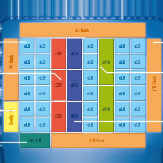
A block diagram of Menta’s fifth-generation adaptive eFPGA IP is illustrated below. The fabric primarily consists of embedded logic blocks (eLBs), embedded DSP blocks (eDSPs), and embedded memory blocks (eMBs), where the eMBs are realized using any third-party RAM technology of the developer’s choosing. Furthermore, designers can also add their own embedded custom blocks (eCBs) into the mix.
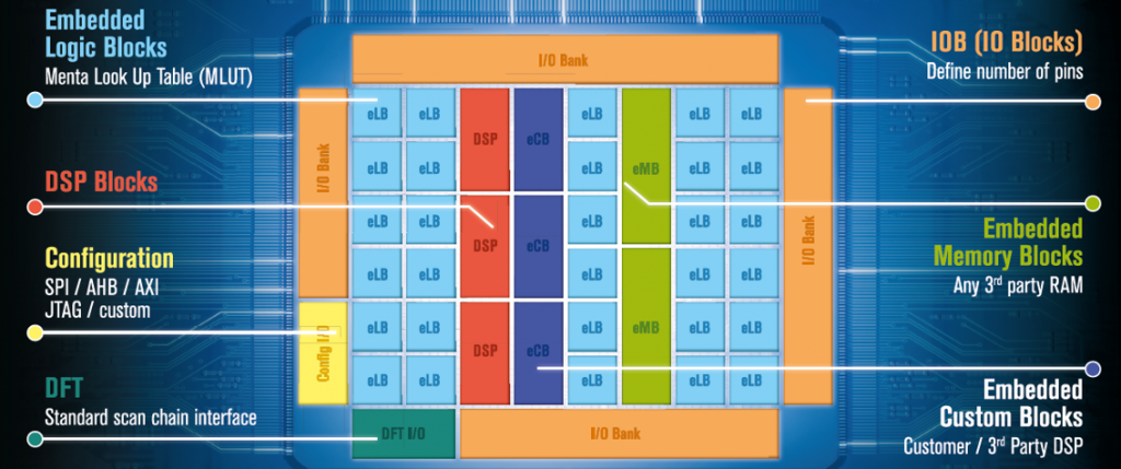
Block diagram of Menta’s fifth-generation adaptive eFPGA IP (Image source: Menta)
Very importantly, developers can select the exact mix of eLBs, eDSPs, eMBs, etc. they wish to employ in their programmable eFPGA fabric. One clever point is that Menta’s Origami development tools can analyze the design’s RTL and provide an estimate as to how many cells of different types the design will require.
As another aside (I can’t help myself — it was the fact that Menta’s development tools boast the “Origami” moniker that made me do it), my old high school chum, Nick Robinson, has written over 80 books on origami and, in 2004, was awarded the Sydney French medal in 2004 by the British Origami Society. But we digress…
Even more importantly, as opposed to 6T (six transistor) SRAM cells, the eFPGA’s configuration cells are implemented as D-type flip-flops from whichever standard cell library the designer is using. The fact that these flops are slightly larger than 6T SRAM cells is compensated by the fact that they don’t require the SRAM’s support logic. Furthermore, this flop-based logic is optimized for reading and writing the configuration bitstream and for implementing design for test (DFT) circuitry (Menta has a patent). Also, they can be used as part of a standard SCAN chain DFT methodology.
With regard to the input/output (I/O) banks shown in the image above, these are simply pins attached to D-type flip-flops, thereby facilitating timing closure for the eFPGA design on its own and in the context of the ASIC/SoC design.
When it comes to the eDSP blocks, I should point out that the chaps and chapesses at Menta actually just call these DSP blocks. However, I think they should be called eDSP blocks to match the overall theme, so that’s what I’m going to use (I’m prepared to stand vigil until the folks at Menta capitulate and follow my lead). In addition to traditional configurable multiplier-accumulator (MAC) functionality, each patented eDSP block also contains a special finite state machine (FSM) and FIR/IIR coefficient function. This is pretty clever. If you want to implement an FIR filter with 32 taps, for example, you either have to use 32 DSP blocks one time, or cycle around using the same DSP block 32 times. In this latter case, when using a regular DSP block, you have to pipe in the coefficients and perform the cycle control externally. By comparison, in the case of Manta’s eDSP block, the cycle control and the 32 coefficients all form part of the eDSP — Genius!
With regard to the eLBs, Menta also uses the term logic cell (LC). Menta’s eFPGA IP is fully scalable from small (S: 100 to 2K LCs), to medium (M: 2K to 6K LCs), large (L: 6K to 60K LCs), and extra-large (XL: 60K to 200K LCs). So, what exactly is an LC? Well, I’m glad you asked, because this takes me back to the days of confusion between “equivalent gates” (in ASICs/SoCs) and “system gates” and logic cells (LCs)/logic elements (LEs) in FPGAs.
In the world circa the 1990s, it used to be common to compare ASIC devices in terms of “equivalent gates.” The idea was to convert each logic function into some number of equivalent gates — such as 2-input NAND gates — and then add them all together so that you could proudly proclaim “Mine is bigger than yours (and so is my ASIC)!”
When FPGAs first appeared on the scene, they offered only low capacity and were not seen as competition for ASICs. Over time, however, FPGAs increased in capacity, eventually becoming large enough to attack some of the designs that would previously have fallen to ASICs. But the LCs/LEs in FPGAs were based on 4-input look-up tables (LUTs or LUT4s), along with some additional logic in the form of multiplexers and flip-flops. So, the problem now became how to compare an ASIC design to an FPGA equivalent.
To cut a long story short, the FPGA vendors came up with a nebulous concept called “system gates,” which allowed them to say “Our FPGA can represent XXX system gates” and “One system gate is equivalent to YYY logic gates.” As I said in my 2010 column, FPGAs: System gates or logic cells/elements?:
In order to address this issue, in the early 1990s, FPGA vendors started talking about “System Gates” Some folks say that this was a noble attempt to use terminology that ASIC designers could relate to, while others believe it was a callow marketing ploy that didn’t do anyone any favors.
The reason I mention this here is that, when the folks at Menta talk about 100 LCs, they are basing this on an LC containing a 4-input LUT (LUT4). And the reason this is confusing is that Menta’s eLBs are actually based on a special patented Menta LUT called an MLUT, which is based on a 6-input LUT (LUT6). So, 100 LCs actually equates to 72 MLUTs/LUT6s. The reason the guys and gals at META do this is that just about every other regular FPGA vendor in this size uses LUT4s and Menta didn’t want to place themselves at a perceived disadvantage (note that the honking big FPGAs from Intel and Xilinx might flaunt LUT7s or LUT8s). On the one hand, I fully understand Menta’s position and I would do this myself if I were they. On the other hand, it’s one more level of indirection that I really didn’t need today (LOL).
In addition to supporting FD-SOI processes, should you wish to use them, Menta also backs many of the techniques discussed in my earlier Handling Radiation in SRAM-Based FPGAs column, including adding delay elements to mitigate against single event transients (SETs) and performing TMR at the register level to mitigate against single event upsets (SEUs).
Menta also supports performing TMR on the whole eFPGA design; that is, generating three identical copies of the eFPGA to be incorporated into the ASIC/SoC, and then using voting circuits on all of the outputs and using the “best two out of three” approach. They even include an option to perform continuous error-correcting code (ECC) checks on the configuration to detect and fix any radiation-induced configuration errors.
Phew! I don’t know about you, but there’s a lot to wrap one’s brain around here. What I do know is that if I were planning on creating an ASIC/SoC, even if I didn’t currently have an application for it, I would definitely consider including some of Menta’s eFPGA fabric in there, “Just in case.” In reality, I think I would also look at implementing appropriate functions in the ASIC/SoC’s using eFPGA fabric, thereby leaving myself with some “wiggle room” to accommodate future changes in requirements and/or specifications. How about you? Do you have any thoughts you’d care to share on any of this?


