


The launch of Sputnik by the Soviet Union on October 4, 1957, was a red flag to the US government. It signaled the USSR’s development of ICBMs that could deliver nuclear weapons across oceans. In response, the US government ramped up its own ICBM program with the completion of the Atlas and development of the Titan missile systems. American Bosch Arma benefitted from those programs by winning the contract to develop an inertial guidance system for the Titan missile, which progressed so quickly that it was retrofitted to the Atlas missile as well. That contract created the opportunity for Edward Keonjian to leave General Electric (GE) in 1957, after having worked there as a transistor application engineer for several years.
What happened next may well have set the course for the development of the integrated circuit. In his autobiography, Survived to Tell, Keonjian writes:
“In 1959 I designed a prototype of an integrated circuit (IC), which represented a full computer adder. Since Arma did not have the ability to manufacture transistors, I asked J.S. Kilby of Texas Instruments to put my primitive IC in a more acceptable form. He did. Thus the first prototype of the integrated circuit was born.”
That account of the making of the first integrated circuit prototype doesn’t jive with the other accounts I’ve read, so I did some research to try to reconcile Keonjian’s account with many other accounts of IC development that I’ve read over the years. First, here’s a description of Keonjian’s visit to Fairchild Semiconductor on January 20, 1959, from the book Moore’s Law: The Life of Gordon Moore, Silicon Valley’s Quiet Revolutionary, written by Arnold Thackray, David Brock, and Rachel Jones:
“On January 20, 1959, immediately following [Jean] Hoerni’s demonstration of his planar process, Gordon Moore, Bob Noyce, and their cofounders were directly introduced to the demand for highly miniaturized circuitry. They were visited by the noted engineer Edward Keonjian. Keonjian was heading American Bosch Arma’s computer project for the Atlas intercontinental ballistic missile. As Arma had already ordered sample quantities of Moore’s NPN mesa [transistor], this visit was high stakes. Keonjian filled them in on his activities. His team’s computer would incorporate ‘microminiature circuits.’ Since Arma did not have the capability to make military-grade diffused silicon transistors to plug into its circuits, Keonjian proposed to ship his printed ‘plates’ to Fairchild Semiconductor. They would make mesa transistors and put them into the printed circuits. Keonjian requested a quote for this work, ‘ASAP.’”
It’s clear from this passage that Keonjian envisioned the manufacture of hybrid circuits. Here’s another account of that same meeting, as described in a book titled Makers of the Microchip: A Documentary History of Fairchild Semiconductor:
“An event that may have animated Noyce’s interest in microcircuitry was a visit to Fairchild Semiconductor by Edward Keonjian on 20 January 1959, three days before Noyce wrote this entry in his patent notebook. Keonjian was a senior engineer at the American Bosch Arma Corporation, a manufacturer of military avionics based in New York. At American Bosch Arma, he directed the design of a miniaturized guidance computer for the Atlas missile. The Atlas – the first American ICBM – was developed in a ‘crash program’ by the military and its contractors in the second half of the 1950s. A major focus of Keonjian’s Atlas computer project was the development of miniature circuits, especially hybrid circuits, for the central processing unit. Keonjian had designed miniaturized hybrid circuits for the project, but American Bosch Arma lacked the knowhow to fabricate the required transistors. Keonjian was looking to collaborate with a firm that had such silicon manufacturing capability. During his visit to Fairchild Semiconductor, Keonjian talked with the founders about “microminiaturized circuits,” especially a full adder that he was developing for his airborne digital computer. A full adder is a logic circuit that performs addition operations. Keonjian discussed the possibility of working with Fairchild Semiconductor on the production of these hybrid circuits.”
This paragraph immediately leads to the question, what was the entry that Noyce entered into his patent notebook? That question is answered in an article co-authored by noted technology historian Michael Riordan and my friend, technology historian, and curator at the Computer History Museum, David Laws. In their article titled “Making Micrologic: The Development of the Planar IC at Fairchild Semiconductor, 1957–1963”, Riordan and Laws write:
“On 23 January, three days after Keonjian’s visit, Noyce wrote an entry in his lab notebook entitled ‘Methods of Isolating Multiple Devices’ that included the design of a full adder. It begins, ‘In many applications now it would be desirable to make multiple devices on a single piece of silicon in order to be able to make interconnections between the devices as part of the manufacturing process.’ He proceeded to show how a full adder could be fabricated on a single chip from a matrix of diodes by using ‘the SiO2 layer as an insulator to isolate contact strips from the underlying silicon.’ Noyce also noted that the techniques could be applied ‘to transistors as well as diodes . . . (to build) a generalized logic element’ and included a schematic for a logic adder circuit.”
However, Keonjian’s autobiography discusses meetings with Jack Kilby at Texas Instruments (TI), not Moore and Noyce at Fairchild, so here’s another account from a different article titled “The Early History of ICs at Texas Instruments: A Personal View,” written by Charles H. Phipps, who worked for TI for 30 years starting in 1957:
“After joining TI in May 1958, Kilby immediately sketched out an idea for a new form of modular circuit assembly. In it, circuit components including transistors would be made in a standard cylindrical form and inserted into printed-circuit-board assemblies. Kilby worked with others at TI to fabricate prototype tubular transistors and to make experimental circuits using them. During the annual TI vacation period in July, Kilby kept working because he did not yet qualify for vacation. Working undisturbed, he came to the conclusion that his and other modular assembly approaches would not make a big impact on the circuit cost problem. Instead, Kilby considered an all-semiconductor approach.
“In his laboratory notebook, on 24 July 1958, he wrote, ‘Extreme miniaturization of many electrical circuits could be achieved by making resistors, capacitors, and transistors & diodes on a single slice of silicon.’ This was the idea of the semiconductor IC. He then sketched an oscillator circuit formed in situ in a semiconductor substrate. After employees returned from vacation, Kilby reviewed his concept with Adcock and a working model of an analog oscillator circuit was fabricated in September 1958, followed by several digital logic circuits in early fall.”
These events at TI, as described in Phipps’s article, occur in 1958, several months before Keonjian made his journey to find a semiconductor partner for his hybrid circuits. And yet, it’s clear that Keonjian spoke with Kilby because the two men co-authored a paper titled “Design of a Semiconductor-Solid-Circuit Adder” for the 1959 International Electron Devices Meeting (IEDM). A four-paragraph summary of this paper appears in the 1959 IEDM Conference Proceedings, which says: “The circuit consists of 17 individual circuits, seven amplifiers, eight ‘And’ circuits, and a flip-flop.” A far more detailed description of Keonjian’s full adder appears with photographs of prototype implementations in an article titled “Microminiaturizing A Space Vehicle Computer,” which appeared in the April 29, 1960, issue of Electronics Magazine. Here’s the block diagram of the full adder from that article:
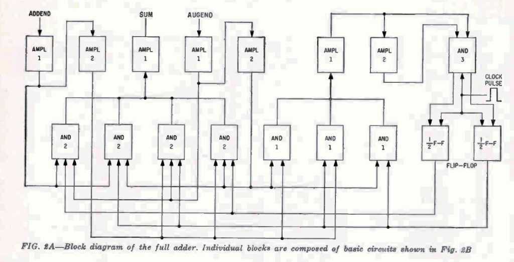
Functional block diagram of Edward Keonjian’s 1-bit full-adder circuit. Image credit: Electronics Magazine
According to Keonjian’s article, “Seven amplifiers, eight AND circuits, and one flip-flop comprise 17 individual circuits which are fabricated on 13 wafers. Each wafer is 0.5 by 0.5 by 0.03 inch.” Note that the adder includes a latch to store one bit but lacks a carry bit. The article’s lead image shows the 1-bit full-adder prototype assembly, which consists of 13 stacked ceramic wafers connected by hand-soldered wiring:
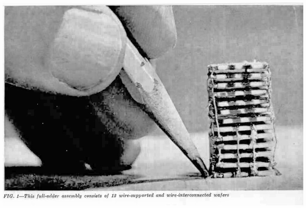
Prototype realization of Edward Keonjian’s full-adder circuit in hybrid module form. Image credit: Electronics Magazine
As you can see from the above image, Keonjian’s 1-bit full-adder prototype device is a hybrid module and is clearly not a monolithic integrated circuit or anything close to an IC. This module’s stacked-wafer construction looks very much like the miniaturized electronic module development efforts of the day, including Project Tinkertoy at the US National Bureau of Standards, funded by the US Navy, and the RCA Micromodule project, funded by the US Army Signal Corps. (See “The Semiconductor Company from Another World: The Siliconix Story, Part 3 – Molecular Electronics.”)
It makes sense that Keonjian’s 1-bit full-adder prototype was realized as a hybrid module in 1959. Based on the individual function block schematics provided by Keonjian’s 1960 article in Electronics, his 1-bit full adder circuit required 85 electronic components, including resistors, capacitors, diodes, and NPN transistors. No semiconductor company could manufacture a monolithic device with that many integrated electronic components in 1959.
The initial commercial ICs offered by both Fairchild Semiconductor and TI were individual flip-flops, which are the functional equivalent of just two of the 17 function blocks in Keonjian’s full-adder circuit. Fairchild Semiconductor would advertise a “Type H” half-adder IC in its μLogic IC family by 1960, but it consisted of three gates and had a carry bit but no storage latch. In fact, Fairchild Semiconductor’s Gordon Moore wrote the chapter on integrated circuits for Keonjian’s book, Microelectronics: Design, Theory, and Fabrication, published in 1963. That chapter contains an image that shows the members of the μLogic IC family circa 1963, when the book was published. The image provides a detailed look inside these ICs:
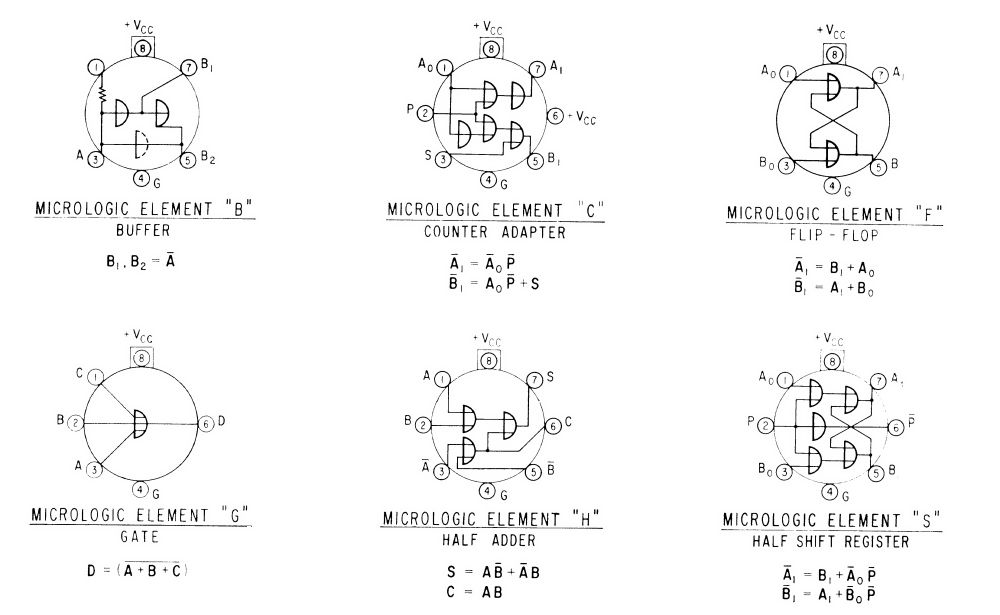
Fairchild Semiconductor’s μLogic IC family circa 1963. Image credit: Microelectronics: Design, Theory, and Fabrication, McGraw-Hill Book Company
Based on the original list of five ICs that Gordon Moore used to develop the Moore’s Law curve in 1965, plus two extra ICs, as described in my article titled “Moore’s Law and the Seven Devices,” Fairchild Semiconductor would not offer a commercial IC based on its planar manufacturing process that incorporated as many as 85 electronic components until 1965, at the earliest.
It certainly appears that Keonjian’s discussions with Fairchild Semiconductor and TI helped to spur IC development at those companies by proving that military contractors would be vitally interested in such devices. It also appears that Keonjian continued to hold a hybrid-module mindset, which is not surprising considering that 1958 and 1959 were the very first years of IC development. In fact, a report titled “Survey of Microminiaturization of Electronic Equipment” and prepared for the US Air Force Ballistic Missile Division by Space Technology Laboratories, published at the end of 1959, focuses mainly on hybrid circuit manufacturing, and barely delves into the very early IC development at Fairchild Semiconductor and TI. IC technology was not yet ready for prime time in 1959.
In any case, Keonjian’s discussions with the leading-edge thinkers in hybrid circuit and IC development throughout the electronics industry on behalf of American Bosch Arma set him up for his next big role, that of microelectronics ambassador with portfolio to the worldwide electronics industry on behalf of American Bosch Arma, followed by similar positions with Grumman, NATO, and the United Nations.
References
Edward Keonjian, Survived to Tell, Sunstone Press, 1997, p 175
Edward Keonjian, “Microminiaturizing A Space Vehicle Computer,” Electronics Magazine, April 29, 1960, pp 95-98
Edward Keonjian, Microelectronics: Design, Theory, and Fabrication, McGraw-Hill Book Company, 1963, p 334
Arnold Thackray, David C. Brock, and Rachel Jones, Moore’s Law: The Life of Gordon Moore, Silicon Valley’s Quiet Revolutionary, Basic Books, 2015, p 201
Christophe Lecuyer and David C. Brock, Makers of the Microchip: A Documentary History of Fairchild Semiconductor, The MIT Press, October 25, 2022, pp 156-157
David Laws, “Who Invented the IC?,” August 20, 2014, Computer History Museum blog
David Laws and Michael Riordan, “Making Micrologic: The Development of the Planar IC at Fairchild Semiconductor, 1957–1963,” IEEE Annals of the History of Computing, January-March 2012, pp 20-36
- V. Horton and T. D. Smith, “Survey of Microminiaturization of Electronic Equipment,” Space Technology Laboratories, December 31, 1959


