

After spending five years at the DH Baldwin Piano company developing photocells for optical encoders, Bill and Frances Hugle were ready for a new challenge. According to family records, Bill left for Youngwood, Pennsylvania outside of Pittsburgh in 1958 to help Westinghouse set up a new cleanroom at its semiconductor fab in that town. Frances followed with their four children in February 1960. However, the Hugles would not stay in Pennsylvania for long. By the end of 1960, they’d relocated to Thousand Oaks, California – putting them closer and closer to Silicon Valley.
Big things were happening to Westinghouse in 1958 when Bill Hugle started working at the company’s Youngwood facility outside of Pittsburgh, Pennsylvania. Miniaturization was the name of the game at the time, and the US Air Force had gotten very excited about “Molecular Electronics.” The quest for miniaturization started in the early 1950s with Project Tinkertoy, conducted by the US National Bureau of Standards and funded by the US Navy. Not to be outdone, the US Army Signal Corps funded the Micromodule (or “Micro-module”) program at RCA. Project Tinkertoy was based on tube technology, while the Micromodule program was based on discrete transistors. Both programs sought to develop automated methods for manufacturing small, reliable electronic modules built from stacks of miniature ceramic circuit boards and discrete electronic components.
The US Air Force dreamed even bigger, adopting ideas introduced by MIT Professor Arthur von Hippel, who proposed the development of solid blocks of matter that would implement electronic functions. Professor von Hippel suggested that complex electronic functions could be built from single physical structures using ‘‘molecular engineering.’’ Instead of using prefabricated electronic components such as tubes, transistors, resistors, capacitors, and inductors, von Hippel suggested that it should be possible to build functional devices starting with individual atoms and molecules.
Professor von Hippel’s “Molecular Electronics” concept resonated with the semiconductor executives at Westinghouse, and the company started to work with the US Air Force in 1957, with an eye towards snagging a development contract. With today’s hindsight, it’s readily apparent that integrated circuits precisely fit von Hippel’s description, but the integrated circuit wouldn’t be invented until 1959, so that’s not the initial direction taken by Westinghouse for the US Air Force.
Westinghouse, an early licensee of the Bell Labs transistor patents, was already producing ultra-pure and single-crystal silicon ingots to manufacture semiconductors, with an emphasis on power rectifiers and power transistors. The Molecular Electronics program was seen as an extension of this work.
George C. Sziklai, an engineer on the staff of Corporate Vice President of Engineering John A. Hutcheson, initiated a program to evaluate von Hippel’s Molecular Electronics concept. The program plan included ideas for a block that would convert 110 volts ac into 9 volts dc using the Seebeck thermoelectric effect and another block that would implement an RC time-delay circuit by exploiting a capacitive interface between two different resistive materials.
Representatives from Westinghouse met with Air Force Cambridge Research Center staff at Hanscom Air Force Base near Bedford, Massachusetts, to present their ideas for molecular systems engineering, and the visit generated interest from several military branches. To continue the momentum, Westinghouse established a Solid State Advanced Development Laboratory at the Youngwood Semiconductor Division to pursue molecular electronics technology. That was 1958, the same year that Bill Hugle went to the Westinghouse Youngwood plant to help set up a clean room.
In February 1959, Westinghouse’s Solid State Advanced Development Laboratory submitted a ‘‘Proposal for Molecular Electronics: Dendritic Approach’’ to the US Air Force’s Aeronautical System Center of the Air Mobility Command at Wright-Patterson Air Force Base in Dayton, Ohio. The proposed manufacturing process would grow a continuous germanium ribbon that would allow for fabricating transistors and other devices at a rate of 6 to 12 inches per minute. The yield for this “transistors-by-the-inch” fabrication process was optimistically projected to be “very near 100%.’’ Westinghouse’s Seymour W. Herwald predicted that the dendritic approach would make it possible to automatically produce functional electronics blocks, such as radio receivers and amplifiers, on a continuous semiconductor ribbon starting from a pool of molten germanium. Westinghouse’s proposal won a $1.6 million development contract from the US Air Force in April 1959.
In March 1959, John D. Husher, a recent BSEE graduate, joined the Youngwood Semiconductor Division’s Advanced Development lab. He became intrigued by the idea of producing four transistors from a single power transistor die by making a shallow cut through the transistor’s upper base and emitter layers to create isolated semiconductor islands that would function as four separate transistors with a common collector. Working on the project during lunch breaks, Husher built a carrier for a power transistor die from a stainless steel plate, fixed a power transistor die to the carrier, and blasted it with walnut shells to cut the large transistor into four smaller transistors with a common collector. Husher then realized that he could also fashion resistors and capacitors from the same raised islands and that he could use gold wires to connect all these components together to create a complete electronic circuit on one die. This work seems to lie in a zone somewhere between Jack Kilby’s hand-wired IC concept at Texas Instruments and Robert Noyce’s planar IC concept at Fairchild Semiconductor.
Husher developed a few designs using this technique including an audio amplifier, high-gain Darlington transistor pairs, and a video amplifier. His manager, Herbert Henkels, recognized that Husher’s idea met the molecular electronics program’s objectives. Henkels arranged to borrow a private plane from a friend of his, golfer Arnold Palmer, and flew from Pennsylvania to Wright-Patterson Air Force Base to meet with managers at the Air Force Electronic Technical Laboratory. There, he and Husher presented the handcrafted devices as prototypes of a new Westinghouse research program to build Functional Electronic Blocks (FEBs). Within a couple of months, ETL redirected molecular electronics contract funds to further develop Husher’s FEB manufacturing approach. Husher then designed and fabricated additional FEBs including single-conversion radio receiver circuits and a single-chip IF amplifier.
In a January, 1960 meeting with the US Air Force’s Air Research and Development Command at Andrews Air Force Base in Maryland, Westinghouse presented eight devices produced for the Molecular Electronics development contract:
· A five-watt, directly cascaded audio amplifier
· A two-stage video amplifier
· A frequency selective amplifier with notch filter in a feedback loop around the amplifier structure
· A variety of multivibrators including bistable [flip-flop], monostable [one-shot], and astable [oscillator]
· A variable potentiometer based on the logarithmic addition of two inputs
· A variety of multiposition semiconductor switches (including an “OR” switch, a multiple NPNP Dynistor switch, and a multiple NPNP Trinistor switch with firing electrode)
· An analog-to digital converter employing an NPNP relaxation oscillator
· A two-stage Peltier cooler for cooling infrared detectors to the proper operating temperatures.
Only the Peltier cooler was fabricated as a molecular electronics device as portrayed in the original proposal. Seven of the eight devices were not molecular electronics devices. The audio amplifier integrated multiple interconnected diffused transistors fabricated on a common substrate. The other devices employed Husher’s fabrication techniques. An image of three Molecular Electronics devices appeared in an article published in the May, 1960 issue of “Westinghouse Engineer”:
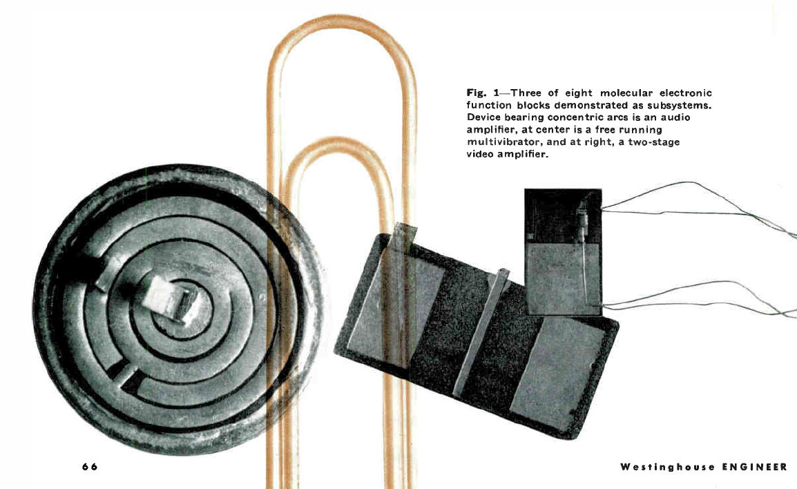
Molecular Electronics Functional Electronic Blocks (FEBs) fabricated by Westinghouse in 1960 for the US Air Force’s Molecular Electronics contract. Image credit: Westinghouse
These semiconductor devices look somewhat crude today, but they certainly were cutting-edge electronic devices in 1960. Ignoring the disparate ways that these FEB prototypes were manufactured, the US Air Force granted a $2.6 million funding extension to the original Molecular Electronics program at Westinghouse, and the project continued, but the writing was soon on the wall. The end was near for Molecular Electronics. In 1962, MIT Lincoln Labs selected Fairchild Semiconductor’s 3-input NOR gate integrated circuit to build the Apollo guidance computers, and the fortunes of the integrated circuit based on the planar manufacturing process shot straight up from there.
Westinghouse established a Molecular Electronics Division in 1962, but by 1963, Westinghouse had started lapping and polishing silicon wafers to use as substrates for planar ICs, just like every other semiconductor maker. Westinghouse’s Molecular Electronics Division survived in name for several years, but the division’s commercial and military semiconductor products soon became nothing more than ICs. Westinghouse continued to use the old name for a few more years because the US Air Force liked it and the company simply expanded the meaning of the phrase to include integrated circuits.
The Hugles did not wait around to see the winding down of Westinghouse’s Molecular Electronics program in Pennsylvania. Although the family had moved from New Jersey to Pennsylvania in February 1960, according to family records, by October of that year, they’d moved 2500 miles to Thousand Oaks, California. The question is, why did the Hugles suddenly move from Pennsylvania to the northwest suburbs of Los Angeles? What suddenly drew Bill and Frances Hugle to California in late 1960?
Family records did not provide any clues about reasons for the move, but after some intense Google searching, the Internet eventually yielded a strong possibility. In 1961, Westinghouse opened an Astroelectronics Laboratory for research in molecular electronics, primarily under US Air Force contracts, with a staff of 300. The Astroelectronics Lab was situated in the Rancho Conejo Center for Light Industry, an industrial park designed to attract the explosion of new aerospace companies springing up in southern California during that era. The industrial park was located on the eastern edge of Newbury Park, bordering Thousand Oaks.
A Westinghouse PR photo from 1962 and sold on Ebay some months ago shows a technician working at a clean bench, fabricating a Molecular Electronics device. Fortunately, the auction curation site WorthPoint.com captured the image of the photo from the original eBay listing, cataloged it, and most importantly, captured an image of the caption on the back of the photo:
“NEWBURY PARK, Calif., March 21 – Molecular electronic devices containing detail too small to be visible except under a microscope are created at the Westinghouse Astroelectronics Laboratory here where work on advanced electronic systems for space and defense is underway. Claudia Murray is shown welding pure gold wire one thousandth of an inch thick to silicon in a solid state device. The gold conducts electricity to or from the device. The technician’s hands work inside a plastic hood where the air is dust free and temperature and humidity are controlled.”
Bill Hugle did not work at Westinghouse alone. Family records and Frances Hugle’s obituary confirm that she also worked for Westinghouse in both Pennsylvania and California and was involved with both semiconductor production and design. The move to Thousand Oaks, near a Westinghouse facility dedicated to the development of Molecular Electronics, strongly suggests that the Hugles were involved in the Westinghouse Molecular Electronics program. However, the Hugles’ stay in southern California was to be long-lived.
Within a year, Bill and Frances Hugle had moved to Silicon Valley, to start a semiconductor company. By working at Westinghouse, first in Pennsylvania and then in southern California, the Hugles had finally absorbed enough technical skills to become chipmakers. Along with their acquired business acumen and connections, gained from starting and joining several technology companies, Frances and Bill Hugle were now ready to start their first semiconductor company: Siliconix.
Note: This history of Frances and Bill Hugle is sparsely documented on the Internet, and this series of articles would not have been possible without the aid and assistance of the Hugles’ grandson, Jake Loomis, and the founder of TechSearch, Jan Vardaman, who was instrumental in creating an IEEE Scholarship program in the name of Frances Hugle, funded in part by Jake Loomis’s mother and Frances Hugle’s daughter, Linda Hugle.
References
The Concepts and Capabilities of Molecular Electronics, Dr. SW Herwald, VP of Research, Westinghouse Electric Corporation, Westinghouse Engineer, May 1960, pp 66-70.
Westinghouse: Microcircuit Pioneer from Molecular Electronics to ICs, Edgar A. Sack and David A. Laws, IEEE Annals of the History of Computing, January-March 2012, pp 74-82.
“Suburban Warriors: The Blue-Collar and Blue-Sky Communities of Southern California’s Aerospace Industry,” Layne Karafantis and Stuart W. Leslie, Journal of Planning History, Volume 18, Issue 1, 2019, pp 3-26.


One fascinating story. I am thankful to Steve Leibson for finding that it was Siliconix that has a connection to DH Baldwin Co. and for resolving the missing links that this former Baldwin Piano and Organ Co. employee (i.e: me) was always intrigued by.