

Microchip previewed its PolarFire 2 mid-range SoC FPGA family at the RISC-V Summit last month in two presentations including a keynote given by Bruce Weyer, the company’s Corporate VP for FPGAs. Although the company provided very few product details, it dropped many hints. So many hints, in fact, that I can give you the information I’ve collected based on these hints, tell you what I think, and let you come to your own conclusions. I’ll give you the “2”s and let you check my math, but then you’ll need to add the “2”s together yourself to get the “4”s. We’ll find out if we’re right in six months or so at this year’s Mi-V conference for Microchip’s RISC-V ecosystem partners for its PolarFire SoC FPGAs.
The original PolarFire SoC FPGA family first appeared in 2017, and then Microchip announced an SoC version of the family with a hardened RISC-V microprocessor core in 2019. (See “Microchip PolarFire Takes a RISC (-V)”) PolarFire is a mid-range FPGA family with 25K to 460K Logic Elements (LEs) and 12.7 Gbps SerDes transceivers, putting it squarely in the mid-range FPGA category.
The SoC members of the original PolarFire family incorporate a multi-core microprocessor subsystem consisting of one SiFive E51 RISC-V processor core and four SiFive U51 RISC-V processor cores all connected through a coherent bus switch to an on-chip, 2-Mbyte L2 cache memory. The PolarFire SoC’s programmable-logic fabric connects to the processor cores over multiple 64-bit AXI4 interface ports through an AMBA switch that’s attached to the coherent bus switch. So far, we don’t know what the PolarFire 2 SoC’s microprocessor subsystem looks like, but Figure 1 shows a block diagram of the original PolarFire SoC’s microprocessor complex. The PolarFire 2 SoC’s microprocessor subsystem will no doubt be bigger and better.
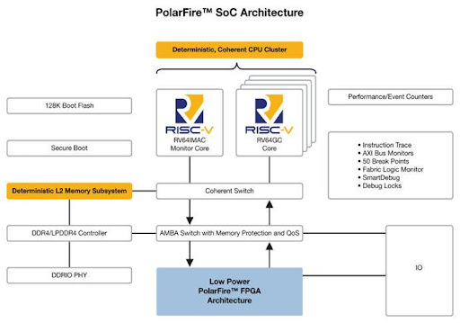
Figure 1: The SoC members of the original PolarFire family incorporate a multi-core microprocessor subsystem consisting of one SiFive E51 RISC-V processor core and four SiFive U51 RISC-V processor cores. Image Credit: Microchip
The SONOS variant of the semiconductor manufacturing process used to fabricate PolarFire FPGAs and SoCs provides the non-volatile memory capability that the original PolarFire FPGA fabric uses for its configuration memory. Because PolarFire SoCs use non-volatile SONOS memory SRAM cells for configuration memory as do mid-range FPGAs and SoCs from AMD/Xilinx and Intel, they’re immune to radiation-induced SEUs (single events upsets), which make them the strongly preferred FPGAs for use in spacecraft. There are Polarfire SoCs flying all over the Solar System at the moment. At least one PolarFire SoC took a ride around the moon on NASA’s recent Orion 1 space mission.
We don’t yet know what process technology Microchip will be using to make PolarFire 2 FPGAs and SoCs, but in its preview of the PolarFire 2 family, Microchip claimed that it would double the power efficiency of the FPGA fabric while also doubling the fabric’s performance. The PolarFire 2 FPGA fabric will again have SEU immunity like the original PolarFire family and it will have “military grade” anti-tamper and cybersecurity features. The company also claimed it would triple the CoreMark benchmark performance of the computing elements on the PolarFire 2 SoCs relative to the performance on the original PolarFire family and would increase the maximum TOPS performance by a whopping 15x. It promised more details would be forthcoming at the company’s Mi-V Summit later this year. Mi-V is Microchip’s RISC-V ecosystem. That’s really about all Microchip said about the new PolarFire 2 family.
A New Process Technology
Although Microchip didn’t provide many details about the Polarfire 2 family, it did drop a lot of direct and indirect clues. As I suggested at the beginning of this article, I can’t guarantee to you that my arithmetic’s correct, so I invite you to add up these clues on your own.
Let’s start with process technology. Some quick Googling took me to a Microchip White Paper titled “PolarFire Non-Volatile FPGA Family Delivers Ground Breaking Value: Cost Optimized, Lowest Power, SEU Immunity, and High-Security” that describes how UMC manufactures the original PolarFire devices for Microchip using a planar 28nm SONOS (silicon–oxide–nitride–oxide–silicon) process technology. SONOS is a process technique that adds non-volatile memory to a chip by inserting a thin, silicon-nitride, charge-trapping layer into an FET’s gate. The charge-trapping layer serves as a memory with two states: negatively charged and positively charged (depleted of electrons, producing holes). Electrons can be moved into and out of this layer using a phenomenon called Fowler-Nordheim tunneling. SONOS semiconductor processes have been around since the late 1970s.
Doubling the power efficiency and performance of PolarFire 2 devices’ FPGA fabric means that Microchip will need to use a more advanced process node. Any node more advanced than 28nm will most likely use FinFETs instead of planar FETs. UMC, Microchip’s current FPGA silicon foundry, has a 14nm FinFET process technology that promises 50 percent less power consumption than its planar 28nm process. However, there’s relatively little information about this 14nm process on UMC’s Web site, so it’s not possible to tell whether that process technology has the non-volatile memory capability needed to produce PolarFire 2 chips.
A little more Googling told me that we’ve known that it’s possible to add a charge-trapping layer to FinFETs (as opposed to planar FETs) using SONOS process steps since 2005, thanks to several authors at TSMC who published a paper on the topic at the IEEE International Electron Devices Meeting held in Washington, DC that year. However, these clues prove nothing. Microchip may not even be planning to use UMC to manufacture PolarFire 2 chips, so you’ll have to put two and two together to decide what sort of process technology Microchip will use to make PolarFire 2 devices. We don’t even know that Microchip will use non-volatile SONOS FinFETs for configuration memory, but the original PolarFire family’s SONOS configuration memory has been successful, so why not?
I think that it’s more likely that the company will stick with SONOS non-volatile memory cells rather than something more exotic like resistive RAM or magnetic RAM because NASA JPL (NASA’s Jet Propulsion Lab) announced last August that it had chosen to partner with Microchip on the closely related HPSC (High Performance Spaceflight Computing) project. Microchip already has plenty of FPGAs, SoCs and other space-ready parts flying around in space, so it’s no surprise that NASA JPL selected Microchip to design and manufacture the HPSC, which is NASA JPL’s attempt to adopt one standardized, multi-core computing platform for all future space projects and to improve existing space-centric computing performance by at least 100x. JPL wants to dip into a global ecosystem for its HPSC processor and wants to draw upon a large pool of programmers who are familiar with a specific processor architecture.
According to Weyer’s keynote, that selection will at least indirectly affect what the PolarFire 2 microprocessor subsystem might look like, because he said that the PolarFire 2 SoC FPGAs will have an HPSC-compatible core complex so that versions of the PolarFire 2 FPGA SoC family can also be used for space applications. Because it’s a NASA project and because NASA likes to fly hardware that’s already flown, exotic non-volatile memories like MRAM and RRAM are less likely to appear on new chips bound for space. Not in the near future, anyway.
Although Microchip provided no direct information about the microprocessor subsystem in the PolarFire 2 SoC FPGAs, the company stashed clues in various places. According to a SiFive press release dated September 6, 2022, the HPSC chip will leverage eight of SiFive’s 64-bit X280 RISC-V processor cores with 512-bit vector extensions and four additional RISC-V cores from SiFive. The SiFive X280 processor cores also incorporate what SiFive calls its “Intelligence Extensions,” which are custom instructions that SiFive developed to accelerate AI/ML operations.
Weyer did not state explicitly that the PolarFire 2 SoC FPGA’s microprocessor subsystem would be based on eight SiFive X280 processor cores plus four more SiFive cores to be named at a later date, like the HPSC, but he did take pains during his keynote to point out that:
- Microchip has been working with SiFive since 2015
- The company offers three RISC-V soft cores in its FPGA library
- The existing PolarFire SoC FPGAs incorporate one SiFive E51 and four SiFive U54 processor cores
- The microprocessor subsystem used in the PolarFire 2 SoC FPGAs will be “compatible” with the HPSC processor ASIC
Once again, you can do the math, but I think it’s pretty clear where Microchip will take the microprocessor subsystem in the PolarFire SoC FPGA. It may have as many instances of the SiFive processor cores as the HPSC, or it may not. We don’t know, yet.
Military-grade Security
Finally, Microchip’s Weyer mentioned that the PolarFire 2 devices will incorporate “military-grade security.” These days, that sort of claim strongly implies the inclusion of post-quantum cryptography, especially for new devices destined to be available for 30 years and designed to last several decades in the field. I fully expect that companies like IBM will have operational quantum computers available for commercial use by then. Post-quantum cryptography is in flux at the moment. NIST (the US National Institute of Standards and Technology) is in the middle of a program to develop, qualify, and adopt new security standards based on post-quantum cryptography. (For more information, see “Looming Crypto Crisis Rides In With Quantum Computing.”)
While Microchip provided no additional details about what it means by military-grade security, another conversation I had at the RISC-V Summit with PQShield’s VP of engineering Graeme Hickey suggests one direction that Microchip might be taking. PQShield is a startup company formed by a group of crypto boffins out of Oxford University in the UK. On June 1, 2022, PQShield announced that Microchip licensed its post-quantum cryptography IP cores “for use in its product portfolio in the coming years.” According to Hickey, PQShield’s post-quantum crypto software library supports all NIST candidates for lattice-based, quantum-safe crypto schemes including Kyber, Dilithium, and Falcon. PQShield’s hardware IP implementation currently supports Kyber and Dilithium and incorporates protection against side-channel attacks.
I particularly asked Hickey about lattice-based, quantum-safe crypto schemes because a different NIST candidate called SIKE (Supersingular Isogeny Key Encapsulation, pronounced “sigh key”), had been broken recently by two people with a laptop computer. Thomas Decru and Wouter Castryck at Catholic University of Leuven in Belgium broke the scheme in a day or two based on a theorem published by the mathematician Ernst Kani in 1997. Scratch SIKE, at least for now.
To get an even better handle on the current state of post-quantum cryptography, I connected with Silvio Dragone, a staff member at IBM Research’s Zurich facility. Dragone published a blog titled “How we quantum-proofed IBM z16,” which appeared last October on IBM’s website. IBM zSystem mainframes have long incorporated cryptographic coprocessor cards called Hardware Security Modules (HSMs), and the IBM z16 mainframe’s HSM contains hardware that implements the CRYSTALS Dilithium and Kyber post-quantum cryptographic algorithm candidates.
Dragone explained that IBM chose to accelerate the z16 mainframe’s HSM with hardware implementations of the Dilithium and Kyber algorithms based on the post-quantum cryptography research done at IBM in Zurich. That research was based on a well-studied mathematical problem and indicated that these algorithms delivered the best performance in the mainframe environment. He said that the beauty of NIST’s post-quantum competition is that it allows the worldwide community of cryptographic experts to analyze these algorithms to tease out any flaws. That’s what occurred with SIKE.
Microchip has not announced what “military-grade security” means within the context of its PolarFire 2 devices, but I’ve provided the clues that I collected at the RISC-V Summit. Once again, I suggest that you can do the math.
The Final Mid-Range FPGA Tally
At the RISC-V Summit, Microchip claimed that the original PolarFire FPGAs are “twice as power efficient” as competing mid-range FPGAs and that PolarFire 2 devices will double that efficiency yet again. You’ll need to evaluate that claim yourself when the tools and chips become available. My experience says that power consumption strongly depends on the design being instantiated in the FPGA. However, Microchip has yet to describe the PolarFire 2 devices, much less fabricate them, so PolarFire 2 must go into the ethereal category of future FPGAs along with several newer mid-range FPGAs that also haven’t yet been built. That category includes Intel’s recently announced Agilex D-series and Sundance Mesa FPGAs and SoCs, scheduled to be made with the Intel 7 process. That’s the process formerly known as 10nm Enhanced SuperFin, 10nm SuperFin++ or something like that; it has changed a few times. (See “Intel Introduces Two Monolithic Agilex FPGA and SoC Families” and “Intel Welcomes You to the Angstrom Era.”)
In another addition to the future mid-range FPGA derby, Lattice Semiconductor recently revealed its mid-range Avant FPGA platform based on TSMC’s 16nm FinFET process technology and the first family based on the Avant platform, called Avant-E. Lattice’s Avant will use the Avant platform to generate multiple mid-range FPGA families. (See “Lattice Strides Into the Mid-Range FPGA Arena With Avant.”)
Honestly, it’s getting pretty crowded in the future mid-range FPGA category, which is great news for future FPGA designs, but it’s hard to compare FPGAs that have yet to appear. Nevertheless, if you look at the collected clues from Microchip’s PolarFire 2 preview announcement, you’ll understand why I am looking forward to Microchip’s formal rollout of the new mid-range FPGA and SoC family later this year. Programmable-logic parts with that much on-chip microprocessor firepower coupled with on-chip, non-volatile FPGA configuration memory and lower power consumption will be compelling for many, many applications, on land, on and under the seas, in the air, and in space.


This article contains no useful information. It’s not as if your investigative work has yielded any usefull information or even hints. They will obviously use more advanced production node, but aboive that, you have nothing. Ie. It might or not be FLASH based etc etc.
Furthermore, you have nothing on Polarfire’s real issues – shitty patched tools, high price and ooold SERDES.
They can do 12 Gbps, but only PCIev2, amongst other things. Paying such $$$ for chip only to connect it to PC through PCIev2 at the time when PCIE5 is out seems blasphemous and locks it out of so many uses.
Some time ago someone asked them on forums why can’t they do multispeed SERDES lanes, so that one could have either, for example one (up to) PCIev5 lane, another that could to PCIev4, anotzher two that could do PCIev3 etc.
This way, one could use modern, fast PCIe versions ( even if narrow) without overloading internal routing or braching the cost ceiling (only one lane is really fast).
MC answered that something like that is in the plans.
BTW, predictions for changes to RISC-V core seem plausible and interesting. I hope they get some more serious core speeds. 600-ish MHz ain’t that great.
BTW, why do all of FPGA manufacturers chomp process advances as their own doing ?
They are to to get into more advanced manufacturing process, which brings certain speed/power advacnes by default. So, why do all of these guys go into great length to show the speedups/powerdowns taht follow natively from a process change ?
This would be easier to swallow if they simply stated what did they managed to achieve above the expected improvement from newer process alone…