


This week at the Intel Innovation event held in Silicon Valley, Intel previewed not one but two new families in its Agilex FPGA and SoC product lines: the Intel Agilex D-series FPGAs and SoCs and a to-be-named FPGA and SoC family formerly known as “Sundance Mesa.” High-end Intel Agilex devices have been fairly successful and, as they often do, customers requested additional Agilex FPGA family members with new features and different characteristics to better fit an even wider range of application requirements.
These new capabilities are increasingly important as customers want to use Agilex FPGAs out towards the network’s edge, and even off the network, where localized processing and analysis are absolutely required. Off the network, the local system must perform the analysis and make decisions because there’s no data center to help out. Even when connected to the network, local processing and decision making help to reduce system-level latency. At the same time, power consumption is at a premium in most edge applications, whether on or off the network, so the implementation technology employed by these applications must consume minimal amounts of power.
Consequently, Intel has rethought the construction of its Agilex FPGAs and SoCs, which were originally built for performance over power considerations. The initial members of the Agilex series are manufactured with chiplet-based hybrid packaging techniques. A central silicon die containing the Agilex FPGA’s programmable logic fabric, manufactured with Intel’s 10nm enhanced SuperFin process, is surrounded with chiplets that add specific I/O features such as fast Ethernet and PCIe SerDes transceivers and CXL. A chiplet stack of high-bandwidth SRAM (HBM) can also be added, as is the case with Agilex M-series devices. Intel’s chiplet-based packaging architecture appears below.
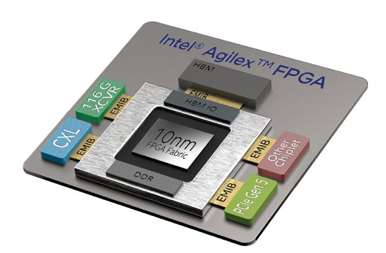
Chiplets buy you flexibility, performance, and time to market. If Intel’s 10nm advanced SuperFin process isn’t right for manufacturing a specific chiplet, and it’s definitely not right in the case of the HBM memory stack, then another process can be used and attached to the central FPGA fabric die. It doesn’t even need to be an Intel process. For example, HBM stacks are not made by Intel but by Micron and Samsung.
However, chiplet-based packaging is clearly more expensive than monolithic semiconductor construction, and it tends to require larger, more expensive packages as well. So, Intel has taken the Agilex D-series and Sundance Mesa devices back to monolithic construction using the Intel 7 process node, which is the new name for Intel’s 10nm enhanced SuperFin process node. Same wine. Same bottle. New label. As you might suspect, the two new Agilex FPGA and SoC families have much in common but there are differences, so let’s take a closer look. This article looks at the similarities among the new Agilex FPGA and SoC families. Part 2 of this article, which appears tomorrow, will discuss the differences.
Perhaps the most important characteristic shared by these two new Agilex FPGA and SoC families and by the entire family of Agilex device families is the second-generation HyperFlex core FPGA fabric architecture. HyperFlex introduces a ton of additional “Hyper-Registers” to the FPGA’s interconnect fabric, as shown below.
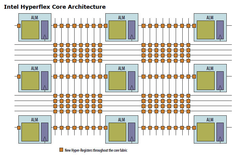
Image credit: Intel
These Hyper-Registers permit the Intel Quartus Prime Software development tools to develop fine-grained clocking and pipelining architectures to really tune your design. Intel claims that Hyper-Registers allow the tools to achieve 47% higher clock frequencies from designs. As with all such performance claims made by FPGA vendors, your mileage may (and probably will) vary.
I first became aware of hyper pipelining, then called “clock concurrent optimization,” when Cadence acquired Azuro back in 2011. Azuro had developed an EDA tool called CCopt that performed “clock-concurrent optimization.” Back then, the concern was that rising design complexity and the use of IP blocks in ASIC design was causing problems with timing closure. That was back in the days of 32nm process technology. Oh, those were the days. Fast forward to today with the Intel 7 process node and the problem now sits squarely on FPGA design’s doorstep.
Clock concurrent optimization merges clock tree synthesis with physical optimization to build complex clock trees while simultaneously optimizing logic delays based on a propagated-clocks timing model. Through this process, clock tree synthesis becomes timing-driven and is tightly coupled with logic placement and sizing. This approach differed from the traditional techniques, which used sequential optimization and skew adjustment across multiple timing paths. For ASICs, this technique requires the insertion of additional registers to adjust skews in clock trees and critical logic paths.
However, this technique isn’t practical for use with FPGAs unless the timing registers are already there to use. There just aren’t enough normal registers in the right place for it. As process technology advanced, it became practical for Intel to insert these registers. If you look at the diagram above, you’ll see that the majority of these registers reside in the FPGA fabric’s switching matrix, where they consume negligible real estate.
Even going back one or two process nodes, the problem of timing closure for complex designs was becoming painfully apparent for FPGAs, which is why Intel introduced the original HyperFlex architecture with the Stratix 10 FPGA family. However, that first-generation HyperFlex architecture introduced some unneeded delays in the hyper-registers, which slowed things down. That’s why Agilex parts got a gen-2 HyperFlex overhaul.
Intel called in a Vogon Constructor Fleet (see “Hitchhiker’s Guide to the Galaxy”) to build a hyperspace bypass inside of each hyper-register so that the signal speeds through the hyper-register if the actual register function isn’t used. Timing results for the second-generation HyperFlex architecture are apparently much improved in the Agilex FPGAs and SoCs, but again I caution you, your mileage probably will vary and you need to test your design with any competing devices to get results that are relevant for your design and your situation.
A second architectural feature shared by the two new Agilex FPGA families is a greatly upgraded DSP block, now upgraded with a fancy new name: DSP with AI Tensor block. That’s title inflation, I’d say. These blocks inherit the design of the variable-precision DSP blocks found in earlier Intel Agilex device families, which already offer some AI capabilities, and they add AI computational features derived from the Tensor block used in the Intel Stratix 10 NX FPGAs.
The DSP with AI Tensor blocks incorporated into the two new Agilex families have two important new operating modes, used for AI/Image/video processing and for DSP-intensive applications that use complex numbers. The first mode is the INT8 tensor mode, which can generate the sum of twenty 8×8-bit multiplications within one DSP/tensor block, a computation that previously required five Intel Agilex FPGA DSP blocks. As shown below, the INT9 vector mode was also enhanced to generate six sums of 9×9 multiplications, which previously needed four Intel Agilex FPGA DSP blocks. These modes are extremely useful for AI-centric tensor math and for various DSP applications.
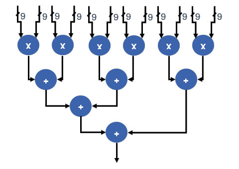
Image credit: Intel
The second new mode, the complex-number mode, doubles the performance of the original Agilex DSP block when performing complex-number multiplication. Previously, two DSP blocks were needed for complex-number multiplication, but the DSP with AI Tensor block incorporated into the two new families of Agilex FPGA and SoC devices can multiply 16-bit, fixed-point, complex numbers within one block.
Both of the new Agilex SoC families also incorporate a significantly improved hard processor system (HPS), which now consists of dual-core Arm Cortex-A76 and dual-core Arm Cortex-A55 processors, a system memory management unit that enables system-wide hardware virtualization, hard memory controllers for various DDR and LPDDR SDRAM families, Ethernet ports, USB ports, I2C and I3C ports, UARTs, SPI ports, timers, and watchdog timers. In addition to the new HPS, both new Agilex device families have additional hard IP cores including hardware support for TSN (time-sensitive networking), AES cryptography, and MIPI D-PHY.


