


I don’t know about you, but I’m starting to feel a little frazzled around the edges, as it were. Things are now progressing so fast that I’m finding it difficult to keep up. I still hear people boasting “We now support PCIe 4.0,” even though PCIe 5.0 is roaming wild and free, and now the folks at Rambus are briefing me on their PCIe 6.0 offerings. Pass me my smelling salts because I’m too young for all this excitement!
Just to ensure that we’re all tap dancing to the same skirl of the bagpipes, let’s remind ourselves that PCI Express (Peripheral Component Interconnect Express), which is abbreviated as PCIe or PCI-e, is a high-speed serial computer expansion bus standard that was designed to replace the older PCI, PCI-X and AGP bus standards. PCIe is now the common motherboard interface for computer graphics cards, hard disk drive host adapters, solid-state drives (SSDs), Wi-Fi and Ethernet hardware connections, and more.
Since its inception, each new release of PCIe has doubled the bandwidth of the previous generation, so no major surprises there. As illustrated below, however, the time between releases reflects an inflection point circa 2017.
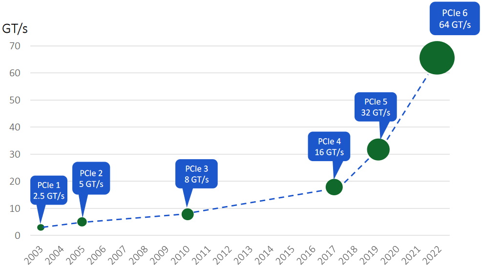
Evolution of PCIe (Source: Rambus)
As we see, PCIe 1.0 was introduced in 2003 with a speed of 2.5 giga transfers per second (GTps). PCIe 2.0 doubled this to 5GTps, and PCIe 3.0, which arrived on the scene in 2010, doubled this again to 8GTps. We then had to wait seven long years for PCIe 4.0 with 16GTps to make an appearance. This marked the beginning of the inflection point I was talking about, because PCIe 5.0 with 32GTps arrived on the scene just two years later in 2019, and PCIe 6.0 popped up three years later in 2022 with 64GTps.
The PCIe 6.0 architecture is going to be essential for system-on-chip (SoC) designers creating next-generation devices that require the movement of large amounts of data within systems, including applications like high performance computing (HPC), cloud computing, artificial intelligence/machine learning, enterprise storage, networking, and automotive, to name but a few.
Furthermore, my understanding is that PCIe 7.0 with 128GTps is anticipated to bid us a cheery “Hello” in 2025, which is just three short years in the future as I pen these words.
Just in case you are not au fait with this topic, the “GT” (“giga transfers”) is standard PCIe nomenclature. On a 1-lane link, 64 giga transfers per second would equate to 64 gigabits per second (Gbps). The thing is that PCIe can range from 1 lane to 32 lanes (in practice most people use 1, 4, 8, or 16), so an 8-lane link running at 64GTps would equate to 8 x 64 = 512Gbps.
I was just chatting with Matt Jones, who is VP of Strategic Marketing at Rambus, which is leading the field with respect to fielding PCIe IP. Matt told me that the reason for the 7-year gap between PCIe 3.0 and PCIe 4.0 was that there wasn’t a killer application or a driving reason to go to Gen 4. But then we started to see an explosion with respect to data generation, movement, and storage—much of which is being driven by the increasing use of artificial intelligence (AI) and machine learning (ML)—which drove Gen 4, followed so quickly by Gen 5, now Gen 6, and soon-to-be Gen 7.
Earlier this year, right around the time of the release of the PCIe 6.0 specification, the guys and gals at Rambus launched their PCIe 6.0 Controller. Just to refresh our memories, PCIe 1.0 through 5.0 used non-return-to-zero (NRZ) signaling, which provides 1 bit per clock. Also, PCIe 1.0 and 2.0 employed 8b/10b (eight bit/ten bit) encoding, while 3.0 through 5.0 employs 128b/130b encoding. By comparison, PCIe 6.0 (and 7.0 to come) uses pulse amplitude modulation 4-level (PAM4), which is a multilevel signal modulation format that provides 2 bits per clock.
Since PAM4 signaling has a slightly higher bit error rate (BER) than NRZ signaling, this drove the need to use forward error correction (FEC). In turn, FEC drove the need to take the protocol from variable-size transaction layer packets (TLPs) to fixed-size packets or flow control units (a.k.a. FLITs) with 242B/256B encoding.
I wondered if the use of FEC would degrade the performance of the system. Matt responded as follows: “Forward error correction does cost you a bit, but there are other mechanisms in play, such as the fact that efficiency is increased in kind by the fixed packet sizes. From an efficiency standpoint, the problem that you have with any number of these protocols is small packets and the overhead versus the payload. With fixed packet sizes, some of that is corrected for, so effectively you’re getting the same throughput.”
The Rambus PCIe 6.0 Controller also supports L0p (pronounced “ell-zero-pee”), which involves dynamic lane allocation to save power. If you have an 8-lane connection between an accelerator and the CPU that are talking to each other via PCIe, for example, you have the ability to lower your bandwidth and enter a power saving mode by performing a “downshift,” if you will, to a 4-lane connection. Later, you can “upshift” back to the 8-lane connection. The underlying mechanism for this has long been available, but it took a lot of steps to implement. Now, things are much more elegant with the introduction of L0p.
But we digress… The reason for the Matt-and-Max chat, and hence for me waffling here, is that the chaps and chapesses at Rambus have just announced the PCIe 6.0 SerDes PHY (physical interface) that goes along with their PCIe 6.0 controller. The complete subsystem that brings these two functions together provides silicon-proven performance to customers who wish to adopt PCIe 6.0.
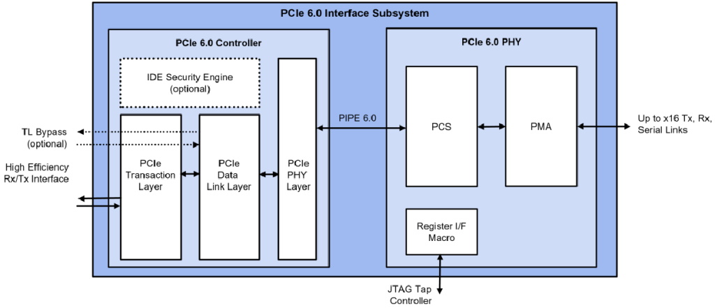
Rambus PCIe 6.0 interface subsystem (Source: Rambus)
In the SerDes/PHY, the physical media attachment (PMA) sublayer performs the serialization and deserialization functions, while the physical coding sublayer (PCS) manages the data encoding and decoding functions.
I should also point out that the PHY block is what we call “hard IP” because it’s process node specific. By comparison, the controller is what we call “soft IP” because it’s delivered as RTL that is synthesizable in any process node and so is process agnostic.
The way to think about this is that PCIe 6.0 comprises an electrical interface (the PHY) and a protocol interface (the controller). The subsystem concept presented here involves taking these two pieces of IP—both of which are extremely complex and high performance—and providing customers (engineers, and system developers) with this integrated solution. This is essentially an “off-the-shelf” PCIe 6.0 solution that allows the folks building leading-edge ASICs and SoCs to focus on their own differentiating content and provides them with a time-to-market (TTM) advantage over their competitors.
Oh yes, and all of this supports the latest and greatest compute express link (CXL) 3.0 standard, but I’m afraid we will have to leave that as a topic for another day. In the meantime, as always, I welcome your comments and questions.


Sorry, but I have a question for Max that is not related to this article. I read max’s Switch debounce series with interest, for example https://www.eejournal.com/article/ultimate-guide-to-switch-debounce-part-4/
In what program are the diagrams and time courses created for this text?
Thanks for the information
Hi there — no worries — I’m just happy to hear that you are reading my columns (as an FYI, Part 9 contains links to all the earlier ones https://www.eejournal.com/article/ultimate-guide-to-switch-debounce-part-9/). Re the diagrams, I create them all in Microsoft Visio — I’m using the old Visio Standard 2010 version (so old it came on a CD 🙂 I think you can get a web-based license of the current version for $5 a month. Also, there are free tools around for this sort of thing, but I really like the way Visio does things and I’ve spent so many hours using it that I really don’t want to learn anything else. I hope this helps.