


AMD has announced an FPGA-based accelerator card with ultra-low-latency Ethernet ports, specifically designed for high-frequency financial trading. Like all such cards, the Alveo UL3524 accelerator card pairs an FPGA with several high-speed, low-latency Ethernet ports, which terminate in four QSFP-DD cages. Each QSFP-DD cage is driven by eight GTF TX/RX transceiver pairs that terminate in the FPGA. The important specification for this card is the low Ethernet transceiver latency, which AMD claims is less than 3ns, which AMD claims is seven times better latency performance than “previous FPGA technology.” In financial technology (fintech) applications like high-speed trading, every added nanosecond of latency translates into profit losses. Big ones.
One significant aspect of the Alveo UL3524 accelerator card is that it’s built around a custom-designed FPGA: the Virtex UltraScale+ XCVU2P. This FPGA incorporates newly developed GTF transceivers with sub-3ns latency. The “previous technology” AMD is using for comparison is the company’s GTY transceiver technology, which is available in several Virtex UltraScale+ FPGAs. (I’m guessing the “F” in GTF stands for “fast.”) However, do not bother to look for the XCVU2P FPGA in the Virtex UltraScale+ product selection guide. It’s not there. The XCVU2P FPGA is currently available only on the Alveo UL3524 accelerator card. The smallest FPGA listed in AMD’s Virtex UltraScale+ product table is the XCVU3P, and neither that FPGA nor any other Virtex UltraScale+ FPGA listed in the table have GTF serial transceivers.
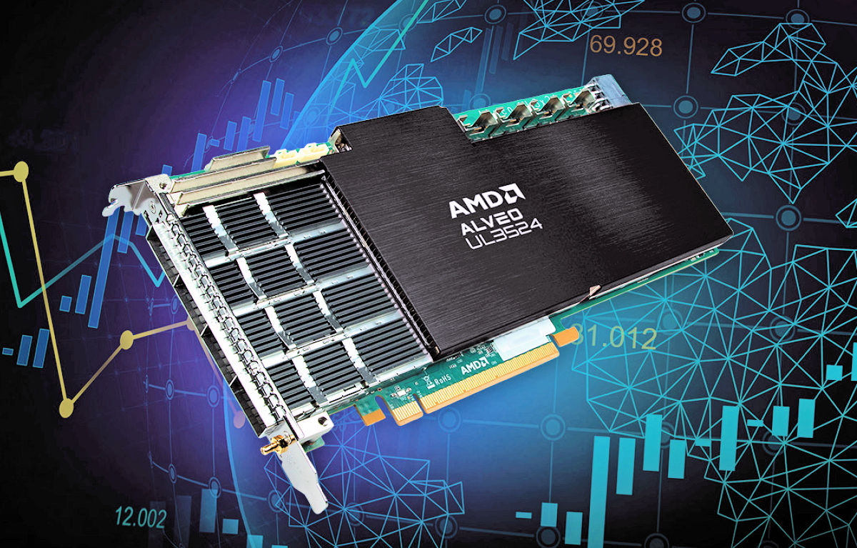
The Alveo UL3524 accelerator card for fintech applications is built around a specially designed FPGA – the Virtex UltraScale+ XCVU2P – which is only available mounted on the accelerator card. Image credit: AMD
Although we cannot discern the XCVU2P FPGA’s specifications from the Virtex UltraScale+ product table, some of its specifications can be found in the Alveo UL3524 accelerator card data sheet and associated collateral. Those specs include:
- 1722K System Logic Cells
- 1680 DSP slices
- 787K LUTS
- 76 Mbits of BRAM
- 180 Mbits of UltraRAM
- 72 GTF serial transceivers (only 64 GTF transceivers are used on the Alveo UL3524 accelerator card)
- 8 GTYP serial transceivers
From the part number, you might expect that the XCVU2P FPGA might have fewer resources than the XCVU3P FPGA, but based on the specs, the new FPGA more closely resembles the Virtex UltraScale+ XCVU7P FPGA in terms of available on-chip resources, except that the XCVU2P FPGA has 63% fewer DSP slices – something that fintech applications apparently do not need.
The disclaimer AMD employs to describe the faster speed of the XCVU2P FPGA’s GTF transceivers is dense, so I provide it here in the name of completeness:
“Testing conducted by AMD Performance Labs as of 8/16/23 on the Alveo UL3524 accelerator card, using Vivado Design Suite 2023.1 and running on Vivado Lab (Hardware Manager) 2023.1. Based on the GTF Latency Benchmark Design configured to enable GTF transceivers in internal near-end loopback mode. GTF TX and RX clocks operate at same frequency of ~644MHz with a 180 degrees phase shift. GTF Latency Benchmark Design measures latency in hardware by latching value of a single free running counter. Latency is measured as the difference between when TX data is latched at the GTF transceiver and when TX data is latched at the GTF receiver prior to routing back into the FPGA fabric. Latency measurement does not include protocol overhead, protocol framing, programmable logic (PL) latency, TX PL interface setup time, RX PL interface clock-to-out, package flight time, and other sources of latency. Benchmark test was run 1,000 times with 250 frames per test. Cited measurement result is based on GTF transceiver “RAW Mode”, where PCS (physical medium attachment) of the transceiver passes data ‘as-is’ to FPGA fabric. Latency measurement is consistent across all test runs for this configuration. System manufacturers may vary configurations, yielding different results.”
In other words, the 3ns latency specification is for loopback operation. The Ethernet protocol stack and any calculations performed for the financial trading algorithms will add to the latency.
There are a few interesting things to glean from this AMD announcement. First, the fintech market appears to be large enough to support the development of a special FPGA just to meet that market’s needs. Second, AMD seems to have decided that the demand for this device will be sufficiently large that it need not sell the FPGA as a piece part and can sell it only as an integral part of the Alveo UL3524 accelerator card. At least for now. At introduction, AMD provided quotes from several fintech vendors that are planning to support the Alveo UL3524 accelerator card including Alpha Data, Exegy, and Hypertec.
I think that it’s interesting that this announcement of a purpose-built, high-end FPGA for fintec applications follows closely on the heels of an unrelated announcement of a purpose-built FPGA that sits at the other end of the FPGA spectrum. I’m referring to the Lattice CrossLinkU-NX FPGA, which I discussed last week. (See “Lattice announces CrossLinkU-NX FPGA with USB 3.2 to Unlock Video Applications.”) Like the AMD Virtex UltraScle+ XCVU2P, the Lattice CrossLinkU-NX FPGA was designed for a specific application. In the case of the AMD XCVU2P, the target application is high-speed financial trading. For the CrossLinkU-NX FPGA, the target application is to serve as a bridge between a high-speed sensor (most likely an imaging sensor for video applications) or set of sensors, and a host CPU with a very specific interface: USB 3.2. However, unlike the Virtex UltraScale+ XCVU2P FPGA, which is a high-end device, Lattice positions the CrossLinkU-NX FPGA as a low-end or “cost effective” FPGA. It’s interesting that the practice of creating FPGAs for narrowly specific applications now appears to work at both ends of the FPGA cost and performance spectrum.
It’s relatively easy to create a new FPGA by modifying an existing one, because FPGA fabrics consist of resource columns (LUTs, DSP slices, BRAMs, etc.) surrounded by peripheral blocks. If you want to change the size of an FPGA fabric, you add or delete columns. If you want to add a new peripheral block, you detach one you don’t want and replace it with the new block, connecting it to the existing wiring in many cases. This is the sort of work that AMD and Lattice engineers needed to perform to create these two new FPGAs.
Last week, I also discussed a new microcontroller (MCU) designed for a specific application. That MCU is the Microchip PIC18-Q20 family of low-end, 8-bit microcontrollers, which specifically target another type of sensor-bridging application. (See “Microchip’s newest 8-bit, 14/20-pin MCU adopts I3C bus for 2-pin interfaces to high-speed devices.”) Unlike FPGAs, semiconductor vendors have been creating application-specific MCUs since they first appeared in the 1970s, and Microchip has a long history of creating such devices.
Despite recent discussions about how expensive IC design has become, I find it telling that companies like AMD, Lattice, and Microchip believe that it’s sufficiently economical to develop new chips for fairly specific applications, once again proving silicon’s flexibility and utility, and, I suspect, underscoring the benefit of highly modular IC design based on well-defined IP blocks.


