


Microchip has just announced the PIC18-Q20 family of 8-bit microcontrollers (MCUs) that feature larger program and data spaces, an I2C peripheral block and one or two I3C peripheral blocks, very low pin counts, and packages as small as 3×3 mm. These devices are available in 14- and 20-pin packages with 16 to 64 Kbytes of on-chip Flash memory for program storage, 1 to 4 Kbytes of on-chip SRAM for data storage, and 256 bytes of EEPROM located in the program-memory address space for non-volatile data storage, including network and security keys and calibration constants. Currently, there are six devices in the PIC18-Q20 family: three in 14-pin packages and three in 20-pin packages. The MCUs in 14-pin packages have just 11 I/O pins and the MCUs in 20-pin packages have 16 I/O pins, which means that pins are at a premium in these devices.
That situation explains the adoption of the I3C interface which is superset-compatible with the I2C bus and its 2-pin interface. However, I3C bus devices use three-state push/pull drivers on the data pin, which permits much faster data-transfer rates than the maximum data rate of 1 Mbps supported by the open-drain drivers employed by the I2C bus. The I3C peripherals in the PIC18-Q20 MCUs, which only operate as Targets, are backward-compatible with the I2C bus, as required by the I3C specification.
This MCU family has integrated level shifters on its I/O pins and supports different I/O voltages for easy interfacing to multiple voltage domains. Some of the MCUs’ I/O pins support 1-volt operation, which makes them compatible with the lowest signal levels used for I3C communications. The I/O level shifters in the PIC18-Q20 MCUs are associated with the Multi-Voltage I/O (MVIO) feature of the device family, and the I/O pins’ output drivers can be powered by the devices’ dedicated VDDIO pins. The 20-pin MCUs have two VDDIO supply pins, and the 14-pin MCUs have one VDDIO supply pin. Drivers on the MCUs’ non-MVIO pins are powered by the devices’ VDD pin. The 14-pin MCUs with 11 I/O pins have two MVIO pins powered by VDDIO2, and the 20-pin MCUs with 16 I/O pins have four MVIO pins, with two of those pins powered by VDDIO2 and the other two MVIO pins powered by VDDIO3.
Because of the faster I3C data rates, low pin counts, integrated I/O-pin level shifters, and numerous on-chip peripherals, including a multichannel 10-bit 300-Ksamples/sec ADC, Microchip is positioning these MCUs as “ideal sensor hubs” that can be used to manage analog, I2C, I3C, and SPI sensors. These MCUs can also serve as I3C-to-I2C bridges and can be used as companion devices for larger MCUs or processors in more complex systems. These sorts of I/O-bridging applications recall the original PIC1650 introduced by General Instrument Microelectronics back in 1975, which was designed as a peripheral controller for the company’s CP1600 microprocessor. (See “A History of Early Microcontrollers, Part 9: The General Instruments PIC1650.”)
A block diagram of the PIC18-Q20 MCU appears below:
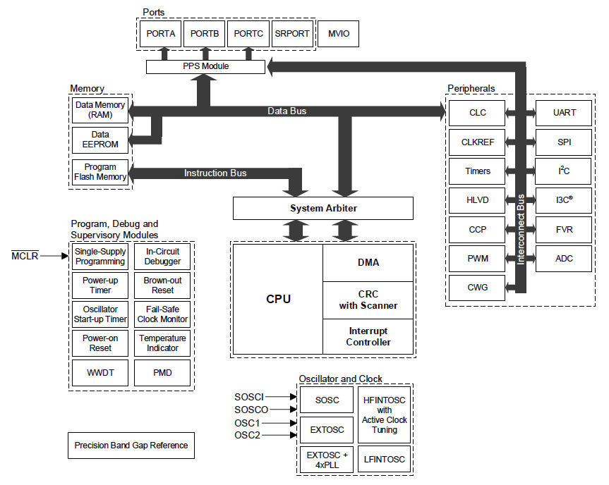
Block diagram of a Microchip PIC18-Q20 MCU. Image credit: Microchip
Microchip’s 8-bit MCUs vary architecturally, but they’re all based on a Harvard processor architecture, which simply means that programs and data reside in different memory spaces. The PIC18 CPU, which Microchip describes as a high-end 8-bit device, has 83 16-bit instructions, incorporates an 8×8-bit hardware multiplier, and can address as much as 2 Mbytes of program memory, far more than can be contained by the on-chip Flash program memory provided in the PIC18-Q20 devices. The PIC18 CPU has a more robust architecture and ISA when compared to Microchip’s low-end PIC10 and PIC 12 and mid-range PIC16 MCUs, and the company says that the PIC18 architecture makes a much better target for C compilers.
As the above diagram shows, the PIC18-Q20 MCUs have a full complement of the peripherals that one might expect to find on a current-generation microcontroller. In fact, it’s obvious that these MCUs have far too many peripheral blocks for the small number of available I/O pins, so some sort of multiplexing and selection scheme is needed. That’s managed by the MCUs’ PPS (Peripheral Pin Select) module shown in the block diagram. Pins on these MCUs can have as many as four different functions. The function in use depends on PPS configuration settings.
Microchip’s announcement of the PIC18-Q20 MCUs provided me with an excellent excuse to delve more deeply into the I3C peripheral bus, which was developed under the auspices of the MIPI Alliance and announced in 2016. I’d been familiar with the 2-wire I2C and 3-wire SPI synchronous serial buses, which appeared on the scene more than 40 years ago, back when I was designing hardware for a living.
The I2C can operate with a maximum 400 kHz clock rate for I2C FM (fast mode) and as fast as 1 MHz for the I2C FM+ (fast mode plus) specification. SPI has no specified maximum serial clock rate but generally operates at or around 1 MHz. Forty years ago, these clock rates were sufficient for the kinds of low-cost chips being connected on these buses. Today, we need faster transfer rates, either to put more peripheral devices on one serial bus or to accommodate newer devices that individually need faster transfer rates, such as MEMS sensors and high-speed ADCs.
The I3C serial bus is much faster than the I2C bus and officially supports 12.5, 25, and 33 MHz serial clock rates while retroactively supporting the I2C 400 kHz and 1 MHz data rates to communicate with legacy devices. However, the I3C peripheral block in the Microchip PIC18-Q20 MCUs supports only the I3C specification’s 12.5 MHz single-data-rate operating mode. Note that I2C devices can operate with clock rates as low as 100 kHz, but the I3C spec does not support clock rates that slow. The PIC18-Q20 MCUs’ I2C peripheral block supports the I2C Host, Client, and Multi-Host operating modes at clock rates of 100 kHz, 400 kHz, and 1 MHz. These MCUs support only the I3C specifications’ Target Device operation and depend on the host MCU or processor to act as an I3C Controller. (The previous Master/Slave designations have been discarded.)
I2C and I3C are multi-drop peripheral buses, and it’s possible to intermix I2C and I3C devices on the same bus if you use the right devices. Some I2C devices already incorporate glitch or spike filters on their clock and data lines. These filters ignore signal pulses smaller than 50 nsec, and, therefore, I2C devices with these filters will ignore the faster I3C traffic on a bus, so there are no compatibility issues. I3C devices do not need or incorporate these filters. It’s possible to add an external glitch filter to a legacy I2C device if needed. You might need to take that approach, for example, if there’s an I2C device you absolutely require in a new design either for reasons of legacy or because there’s no equivalent device available with an I3C interface.
So, what do you think? Would you find one of these MCUs useful in one of your next designs? Let me know in the comment section below.
For another perspective on Microchip’s development of the original PIC microcontroller architecture, see “Steve Sanghi’s new “Up And To The Right” book chronicles Microchip’s journey from nearly bankrupt to Top-20 semiconductor maker.”


