

It’s not often you get to say things like “exponential increase in insatiable demand,” so I’m going to make the most of it by taking a deep breath, pausing for effect, and waiting for the audience’s antici…
…pation to mount. As I’ve mentioned in previous columns (although possibly using different words), we are currently seeing an exponential increase in insatiable demand for increased processing power.
I’m sure we’re all familiar with Moore’s Law, which—if the truth be told—was really more in the way of being a casual observation. Way back in the mists of time we used to call 1965, Gordon Moore, the co-founder of Fairchild Semiconductor and Intel (and former CEO of the latter), posited a doubling every year in the number of transistors that could be fabricated on a semiconductor die. He also predicted that this rate of growth would continue for at least another decade.
In 1975, looking back on the previous decade and looking forward to the next decade, Gordon revised his forecast to a doubling every two years, which is the version most people refer to (although, just for giggles and grins, there are some who opt for a doubling every 18 months).
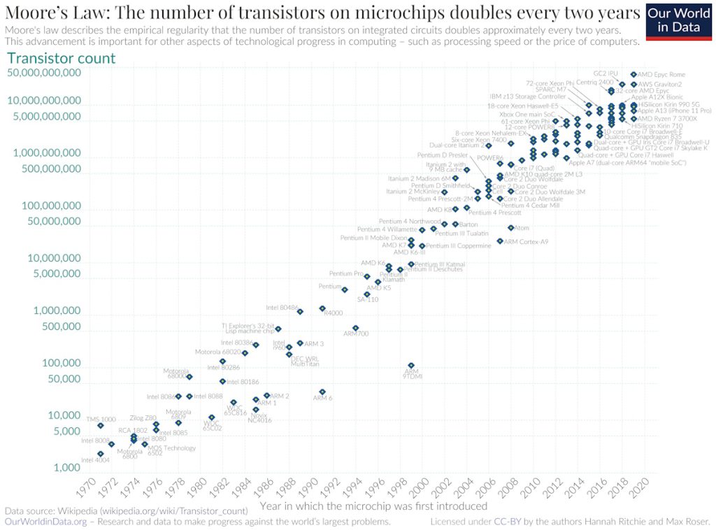
A semi-log plot of transistor counts for microprocessors against dates of introduction shows a near doubling every two years (Source: Wikipedia)
Generally speaking, Moore’s Law has also reflected the amount of computational power provided by microprocessors. At first, this increase in processing power was achieved as a mix of more transistors and higher clock speeds. Later, as clock speeds started to plateau, the industry moved to multiple cores. More recently, we’ve started to extend the multi-core paradigm using innovative architectures coupled with hardware accelerators. And, as for tomorrow, we might reflect on the quote that has been attributed to everyone from the Nobel prize-winning Quantum physicist Niels Bohr to legendary baseball player (and philosopher) Yogi Berra: “It is difficult to make predictions, especially about the future.”
I couldn’t have said it better myself. What I can say is that you can ask me in 10 years and I’ll tell you what happened (and you can quote me on that).
It used to be said that the only two certainties in life are death and taxes. I personally feel that we could add “more umph” to this list, where “umph” might manifest itself as “the exponential increase in insatiable demand* for increased processing power, memory size, communications speed…” the list goes on. (*Once you’ve started saying this, it’s hard to stop.) Having said this, most people gave the impression of being relatively happy with processing capability tracking the Moore’s Law curve (it’s a curve if you don’t use a logarithmic Y-axis on your plot), at least until…
…things like high-performance computing (HPC) and artificial intelligence (AI) came along. As far back as 2018, the guys and gals at OpenAI—the company that introduced us to ChatGPT, which, ironically, no longer needs any introduction (even my 93-year-old mother knows about it)—noted in their AI and Compute paper that AI could be divided into two eras. During the first era, which spanned from 1956 to 2012, computational requirements for AI training tracked reasonably with Moore’s Law, doubling around every two years, give-or-take. In 2012 we reached an inflection point, and the start of the second era, whereby computational requirements started to double every 3.4 months!
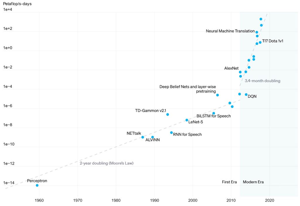
Two eras of computational requirements in training AI systems (Source: Open AI)
Now, you may say “Ah, AI, what can you do, eh?” However, as I noted in an earlier column–Will Intel’s New Architectural Advances Define the Next Decade of Computing?—at Intel’s Architecture Day 2021, Raja Koduri (who was, at that time, the senior vice president and general manager of the Accelerated Computing Systems and Graphics (AXG) Group) noted that Intel was seeing requirements for a doubling in processing power (across the board, not just for AI) every 3 to 4 months.
Now, having humongous computation power is all well and good, but only if you can feed the processors with as much data as they can handle (“Feed me Seymour!”).
Certainly, we can pack mindboggling amounts of Double Data Rate Synchronous Dynamic Random-Access Memory (DDR SDRAM, or just DDR for short) on the same board as the processors, but we are still burning power and adding latency getting data to and from the processors. The current “best in class” solution is to add as much SDRAM inside the chip package as possible, which leads us to High Bandwidth Memory (HBM).
HBM achieves higher bandwidth than DDR4 or GDDR5 while using less power and in a substantially smaller form factor. This is achieved by creating a stack of DRAM dice, which are typically mounted on top of an optional base die that can include buffer circuitry and test logic. One or more HBM stacks can be mounted directly on top of the main processor die, or both the HMB and the processor can be mounted on a silicon interposer.
The reason I’m waffling on about all this is that I was just chatting with Joe Salvador, who is VP of Marketing at Rambus. Joe specializes in Rambus’s interface IP products. In addition to HBM, these include PCIe, CXL, and MIPI IPs.
I must admit that the last I’d looked at HBM, everyone was super excited about the availability of HBM2E, so you can only imagine my surprise and delight when Joe presented me with the following “Evolution of HBM cheat sheet.”
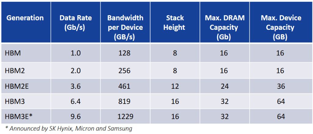
The evolution of HBM cheat sheet (Source: Rambus)
I guess I must have blinked, because I now discover that we’ve already hurled through HBM3 and are heading into HBM3E territory. “OMG,” is all I can say. A stack height of 16 dice and a data rate of 9.6 gigabits per second (Gbps). There’s no wonder this is of interest to the folks building the data center servers that are used for HPC and AI training.
Rambus is a market leader in this sort of interface IP, so it’s no surprise that they’ve just announced their HBM3E memory controller IP. The image below reflects the scenario where the main SoC die and the HBM stack are both mounted on a common silicon interposer, which is not shown in this diagram.
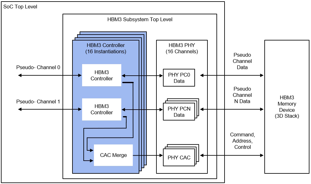
HBM controller block diagram (Source: Rambus)
Why does this image have only “HBM3” annotations as opposed to “HBM3E”? I’m glad you asked. The reason is that the image was created prior to the HBM3E nomenclature being formally adopted as a standard (true to tell, it may still be only a de facto standard at the time of this writing, but that’s good enough for me).
In addition to delivering a market-leading data rate of 9.6Gbps, this latest incarnation of the HBM3 memory controller IP provides a total interface bandwidth of 1,229Gbps (that is, 1.23 terabytes per second (Tbps)) of memory throughput.
All I can say is this will have the HPC geeks and AI nerds squealing in high-pitched voices like… well, things that squeal in high-pitched voices. What say you? Could you use this level of screaming bandwidth in your next design?


Since day one, memory access time has been critical. (because data is accessed randomly)
DDR data rate is only one factor since it reduces the impact on access time for cache misses.
So this just seems like “Gee, what a big number!” (in a squeaky voice, of course!)
Has anyone realistically measured cache hit ratio? I don’t think so… 95% has been ASSUMED in order to
make design tradeoffs of other factors.
The nonsense associated with multicore is malarky because the memory systems cannot deliver data(and instructions) quickly enough.
I don’t think that’s right Karl. Processor designers did not evolve first, second, and third-level caches and multiple cache policies using wet-finger and Kentucky windage methods of engineering. Every application has a different cache hit ratio and processor designers use a basket of target applications to size caches and develop cache policies. The x86 designers have favored Windows applications and server processor designers favor Web applications. There’s indeed a lot of measurement going on with respect to cache policy effectiveness. As for HBM, there’s extensive application-level testing to see if the HBM accelerates code execution, and indeed it does. FPGAs with HBM are very popular with high-performance system designers and they’re not paying the hefty premium for HBM-enhanced FPGAs because they stuck a wet finger in the air. The HBM improves their application performance, measured per application. As for multicore processors, you’re correct in saying that there’s a danger of overloading the memory interface with so many processors. The trick, not always performed perfectly, is to capture the application entirely in a cache. However, even with multicore processors, there’s a lot of testing going on at hyperscalers to discover the optimum number of cores per socket using some sort of price/performance metric for a given basket of target server applications.
Has any of that ever been published for the general masses of idiots like me to peruse?
And how are we to know that the benchmark applications they use have any resemblance to the particular application being developed?
The secret sauce is to design/use a stack based computer to reduce the number of loads and stores and put it on a chip with embedded true dual port memories and forget about caches, hit ratios, DDR, HLS, multicore, etc.
Microsoft did a lot of analysis and concluded that the lowly FPGA can outperform the superscalars.
The report was named something like “Where’s the Beef?”.
No Karl, these studies are not published and are considered proprietary. It’s called “do your own research.” As for stack-based computers, HP during its many love affairs with strange processor architectures briefly fell in love with stack-based machines and implemented the original “classic” HP 3000 minicomputer as a stack machine. As soon as RISC appeared, HP jilted stack machines and fell in love with RISC. Then it was VLIW (Itanium), and we all know how that ended. Love is such a many splendored thing.
I fail to see the justification of primary other than that they can hide the validity of the studies.
No, there are no “benchmark” applications.
And every compiler utilizes a stack and not just for calls. For sure those were failures. However there was FORTH. And now there is C#(Roslyn) API and FPGAs come loaded with embedded true dual port memory blocks…that very few designers know how to use.
And we both remember the “All programmable Planet”, HLS, SystemC, pipelining, FSMs, etc.
And of course RISC vs CISC…which can be anything marketing wants them to be.
“However, there was Forth.” That’s a conversation ender, Karl. I don’t discuss microprocessors or languages as religion.
aw Shucks!
He should be careful at his age taking such long leaps to false conclusions.
More than one of the current compilers use an abstract syntax tree and Roslyn/C# also provides an API. Evaluation of expressions is done using a stack.
Now that he is gone with his proprietary analysis hokum…
The reason for using a stack goes back to Professor Dykstra’s shunting yard algorithm to handle operator precedence. He converted to Reverse Polish Notation while C# uses an AST.
There are Nodes for variables and and values that are issued first so they can be stacked. Then comes binary expressions. Pop 2 operands, evaluate, push result, pop and assign value to variable. All done.
SystemC and HLS are still fumbling in the dark.
Which “He” are we talking about ?– I’ve lost the thread (said Max, sadly)