editor's blog
Subscribe Now

450 In Belgium

Changing wafer size is a big deal. You can kiss all your old equipment good-bye and usher in a whole new suite. So what happens when you’re planning to use that wafer size for a new technology node? You really don’t want to have to have two sets of production equipment, one for each side of the wafer-size shift. But it would also be rough to develop a new wafer size at the same time as developing a new technology node. That’s risk upon risk.

I talked with Ludo Deferm at Semicon West, where 450-mm was all the rage. But this excitement is clearly about things yet to come: there’s not much equipment available yet; only one item – KLA-Tencor’s blank wafer metrology unit – has been announced. And that just ensures that you’re starting with a good blank wafer. The rest is yet to come.

And imec sees 14 nm being the starting node for 450 mm. But the 450-mm R&D facility that imec just got government help for isn’t going to be started until 2014 – you can do the math on when it’s likely to be up and running. So if we had to wait for that before we could develop 14-nm technology, we’d be a long ways away.

As it is, imec is doing 14-nm development work on 300-mm wafers – it’s just that that equipment won’t be used for production. It’s just to get the process itself up. Clearly it will take some freshening up on the new 450-mm equipment when it’s ready. By that time, they’ll already be developing the 10-nm node.

As a curious side fact, he noted that a 200-mm cleanroom is actually more expensive to build than the 450-mm facility. That’s because, back then, the whole room had to be clean. Now everything is sealed in FOUPs, so, while it’s probably not a good idea to be tracking mud into the room or smoking, the level of cleanliness in the room is actually less than it used to be. Inside the equipment, however, there’s little forgiveness for the slightest intruder.

More on the Flemish investment can be found here

Leave a Reply

featured blogs
May 2, 2024
I'm envisioning what one of these pieces would look like on the wall of my office. It would look awesome!...
Apr 30, 2024
Analog IC design engineers need breakthrough technologies & chip design tools to solve modern challenges; learn more from our analog design panel at SNUG 2024.The post Why Analog Design Challenges Need Breakthrough Technologies appeared first on Chip Design....

featured video

Why Wiwynn Energy-Optimized Data Center IT Solutions Use Cadence Optimality Explorer

Sponsored by Cadence Design Systems

In the AI era, as the signal-data rate increases, the signal integrity challenges in server designs also increase. Wiwynn provides hyperscale data centers with innovative cloud IT infrastructure, bringing the best total cost of ownership (TCO), energy, and energy-itemized IT solutions from the cloud to the edge.

Learn more about how Wiwynn is developing a new methodology for PCB designs with Cadence’s Optimality Intelligent System Explorer and Clarity 3D Solver.

featured paper

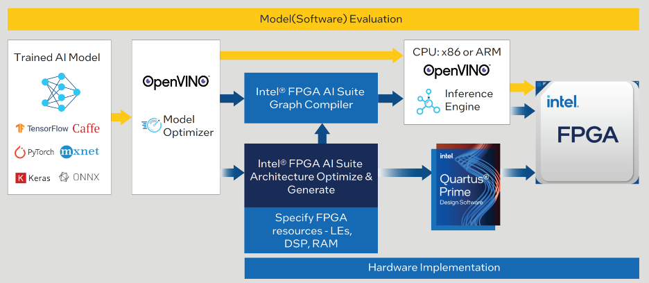
Altera® FPGAs and SoCs with FPGA AI Suite and OpenVINO™ Toolkit Drive Embedded/Edge AI/Machine Learning Applications

Sponsored by Intel

Describes the emerging use cases of FPGA-based AI inference in edge and custom AI applications, and software and hardware solutions for edge FPGA AI.

Click here to read more

featured chalk talk

Achieving High Power Density with IGBT and SiC Power Modules
Sponsored by Mouser Electronics and Infineon
Recent trends in the inverter market have made high power density, scalability, and ease of assembly more important than ever before. In this episode of Chalk Talk, Amelia Dalton and Abraham Markose from Infineon examine how Easy & Econo power modules from Infineon can help solve common inverter design requirements. They explore the benefits and construction of these modules and how you can take advantage of them in your next design.
May 19, 2023
38,680 views