

It’s that time of year again. The SPIE Advanced Lithography conference has come and gone, and the time has come for our annual update on EUV technology, along with directed self-assembly (DSA). Gone are the days of big news for either of those categories. Which means there’s lots of little news of the update variety.
Let’s start with basic stats for EUV. They represent a litany of the things that need improvement as we move towards full production in high volume. Much of this comes from a conversation I had with ASML. If you’re new to this scene, they are the only game in town for the scanners that take all of the diverse bits of challenging EUV technology and bring them together in a giant box that will sit on the production floor. (One of which I got to see in person at Imec last year… through glass, of course… They wouldn’t let me drive it…)
Power and Throughput
Top of the list are source energy and the closely related throughput goals. The lower the power, the longer each exposure has to be to get the right number of photons delivered, and long exposures mean you can’t get as many wafers exposed per hour. Power is steady at 250 W; throughput on existing scanners is about 90 wafers per hour (wph), but they’re being upgraded to 125 wph with an improvement to the drive laser.
That last bit is worth some explanation. You may recall that these units consist of drops of molten tin that are hit mid-air with a laser (actually, twice – once to puff up the drop and increase the surface area, the other to obliterate it with extreme prejudice). That laser pulse was creating some echoes that messed with the target droplet. They did something akin to impedance matching to eliminate (or reduce) the echoes. Doing that in a way that could be incorporated as an upgrade to existing machines was a challenge in itself.
Looking forward, they’ve shown source power as high as 375 W on a new system that’s a few years out. They expect a 300 W spec in production in 2020. As to throughput, deep UV (DUV – aka 193i) does 275 wph. If EUV can get to that level, then ASML suggests that throughput can take a back seat to photon dose – which will help such challenges as line-edge (or line-width) roughness (LER/LWR).
Scanners Hit the Streets
The current ASML scanner is the 3400, of which they’ve produced 15 and shipped 10 to foundries and IDMs. They’re getting uptime of 80%, which is OK, but not enough. They’re targeting more than 90%.
You may recall the issue of collector hazing – residual tin that clouds the surface of the collector. Since the collector’s job is to reflect the UV light into a beam, hazing shuts that down. With no extra mitigation, the collector can haze in seconds or minutes, meaning you would have to shut the whole unit down to clean the collector pretty much all the time. Which would be ridiculous for production.
The current approach uses a hydrogen purge, which helps, but it isn’t good enough. Tin still gets splattered onto chamber walls, from which it then drips onto the collector. This is what needs to be fixed to get the uptime even higher.
In addition, challenges with the droplet generator were reported last year. This further impacted uptime, but that fix is already in place this year – hazing remains the focus.
Reticles and Pellicles
Powering through other metrics, reticle defectivity has improved. In particular, they’ve cleaned up the area where the wafer is held.
Meanwhile, the pellicle challenge continues. A concern here is the pellicle’s ability to handle high dosage. They know that it can take 245 W, and they’ve simulated that they can handle 400 W. Above that, the pellicles simply break. It’s a temperature thing: they can get as hot as 500 or 600 °C.
High temperatures are an issue because this all happens in a vacuum – there’s no convection to carry heat away. The only way heat can dissipate is through blackbody radiation and through the edge, where the pellicle is mounted. The emissivity of the pellicle – that is, its ability to dissipate heat through radiation – is adequate for today’s temperatures, but perhaps not at higher power levels.
You may also recall that the pellicle needs to be transparent(ish) to the EUV beam since that beam will go through the pellicle, reflect off the mask, and go back through the pellicle to the target wafer. That’s two trips through the pellicle, so any energy that gets absorbed by the pellicle reduces the dose received at the wafer. Right now, transmissivity is still around 80%, and they’re trying to get it to 90%. That will also help to reduce pellicle heating.
There’s also strong emphasis on minimizing the overlay between DUV and EUV scanners. Why would that matter? Because EUV will be used only for some layers. Other layers will be exposed using DUV. Overlay would ordinarily be a concern only from DUV to DUV or EUV to EUV. But because we’ll be mixing and matching, you have to be able to overlay an EUV layer onto a DUV layer (and vice versa). ASML says that the EUV-over-DUV overlay specs are now the same as DUV-over-DUV, making this a checked box.
Finally, the high-NA version that can improve resolution is targeted for production in 2025. It’s not a matter of materials (as so much EUV stuff is), but rather lens design.
Irresistibility
And then there’s the matter of resist. The major incumbent is the chemically amplified resist, or CAR. And work continues to improve CAR performance. But we’ve also looked at Inpria’s metal-oxide resists and at nanoparticle resists in general. Metal oxides are, of course, inorganic. But they’re dispersed into and deposited via an organic medium, so the point of the nanoparticle is to surround the inorganic core with organic ligands to make the nanoparticle soluble in the dispersant.
In fact, it turns out that nanoparticles often clump uncontrollably, so, in the resist keynote, Cornell University’s Christopher Ober noted that creating intentional clusters of nanoparticles returned some control to the game.
One potentially confusing element bears clarification. In a time where metal-oxide resists are in the ascendant, references to metal resists caught my eye. In fact, it was mentioned by Brewer Science that metal resists might be usable as their own hard masks. So… they’re giving up the oxide and going with straight metal cores???
A little thought (which I applied far later than I would like to admit) would suggest that this is probably not the case. Using pure metal as a hard mask would be tantamount to using interconnect as a mask. No, this is still about metal oxides. What’s new is that different metals are being tested – ones that absorb EUV light more strongly. So when you hear references to “metal resists,” it’s best to mentally insert “-oxide” into the phrase.
You might think that that’s all there is to resists, but no: there’s yet one more new twist being applied to this game by a new company called Irresistible Materials. Which sounds like they make stuff that doesn’t resist, but don’t be fooled. They’re working on a new type of organic resist that they call multi-trigger resist.
They say that the issue with standard CARs is that they work well at the center of the exposed area, but, at the edges, the acids released during the process can diffuse into unexposed areas, blurring the edge and contributing to LER, LWR and lack of precision. To mitigate this, quenchers are added that have little effect in the central high-dose area, but that quench the acids in the border low-dose areas.
Irresistible Materials (may I call them IM please? Yes… I’m lazy like that…) has a different approach. Rather than adding a quencher as a separate thing, they’ve built a system that has a strong preference for exposure in high-dose areas and not for low-dose areas.
They do this by splitting the active chemistry into two pieces – kind of like old-style epoxy (or, wait… the McDLT? Two references in a month??). Neither part does its thing alone; they have to work together. A photo-initiator gets each side working, and, where there are lots of photons, there will be lots of activated components cheek by jowl. Those components can therefore interact and yield exposed resist.
At the fringes, where few photons fall, you are unlikely to have an activated version of one component near its counterpart at the same time, and the reaction therefore doesn’t occur. So you don’t get exposed resist in those areas.
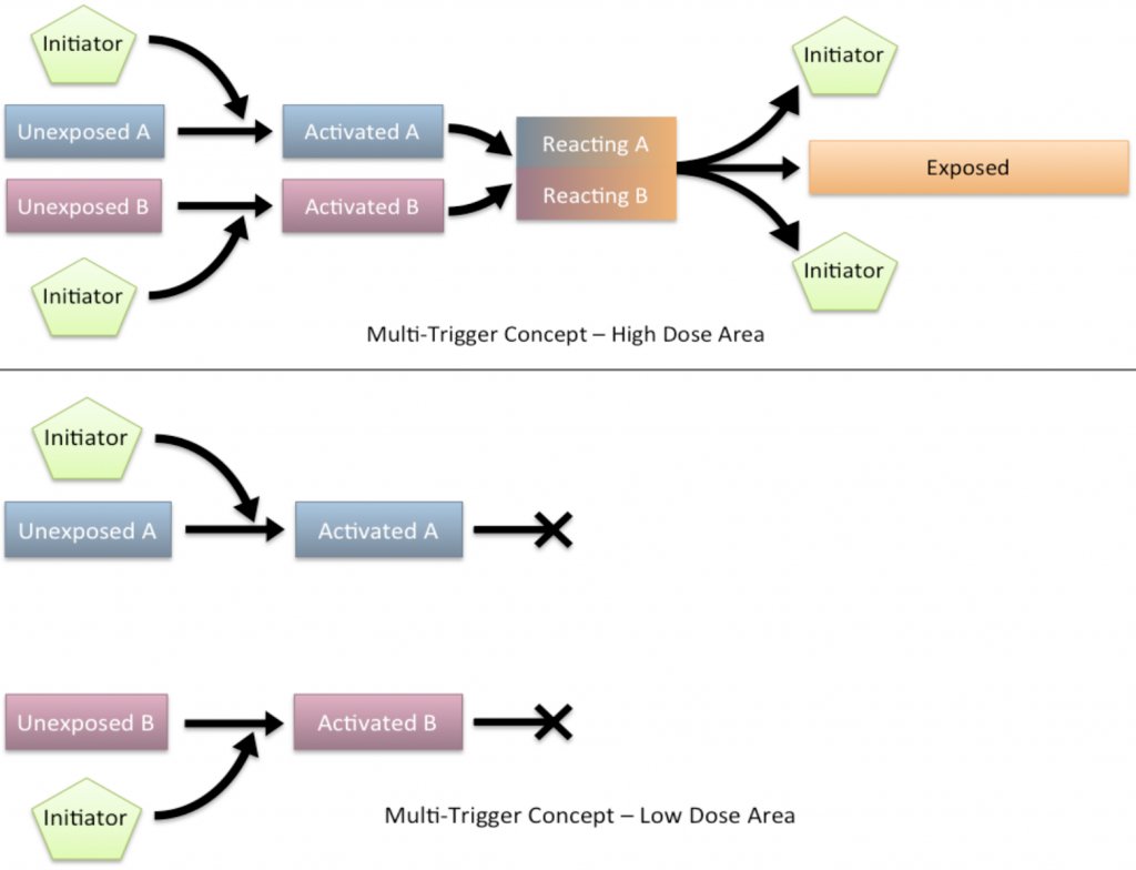
(Image components courtesy Irresistible Materials)
I asked how this compares in performance to metal-oxide resists, and they said that they’re almost up to that level (and getting better). They noted that their versions, being organic, use the same etchants and processing as CARs, making them easier to introduce into an existing fab. They said that metal-oxide resists need different etchants and introduce metals (OK, metal oxides) into fabs, giving them a higher burden of proof before they’ll be widely accepted.
Whatever Happened to DSA?
DSA was such a hot ticket a couple of years ago, and yet you don’t see as much of it lately. It’s not outright gone, and no one has declared it dead, but the energy is definitely more muted. Last year, I heard it explained that defectivity never got to the level required for serious production (which suggested it was moribund if not outright dead).
A discussion with Brewer Science this year suggested a different story. Their assertion is that EUV has sucked all the oxygen out of the room, leaving little to keep non-EUV technologies – and DSA in particular – breathing. They see it as simply a matter of time; when EUV fully hits its stride, then attention can be lavished on DSA again. They look to DSA as an important way to put off the need for SAQP on EUV.
They’re seeing DSA start to replace SADP and SAQP, mostly with contacts and vias. Believe it or not, they’re also seeing attempts at SAOP – octal patterning, although numerous challenges remain there – notably LER (it might work with LER < 1 nm) and pitch-walking.
Brewer Science supplies many of the materials used for both EUV and DSA – which includes the block copolymers (BCPs) that make DSA possible. They obtain their starting BCPs from Arkema and then further refine them to remove ions and side reactants.
They’ve seen DSA defectivity drop by half, although that’s still not enough; more work is needed. They’re also working to improve the etching contrast between the polystyrene on one side of the BCP and the PMMA (poly[methyl methacrylate]) on the other side. They’ve managed features with 7-nm half-pitch, but LER on the guiding structures is still an issue.
So we’ll keep an eye out to see what happens with DSA in the coming years.
[Article was updated to change “energy” references to “power” with respect to EUV sources.]
More info:
SPIE AL EUV Resist keynote: “EUV photolithography: resist progress and challenges”, C. Ober et al, Proc. of SPIE Vol. 10583 1058306-1


What do you think of the current state of EUV and DSA?