feature article
Subscribe Now

EE Journal Live Coverage of NY World Maker Faire 2017

The EE Journal team went to World Maker Faire!

We live tweeted the event @EEJournalTFM as we made our way through the tents to check out the over 750 maker projects at this year’s Faire at the New York Hall of Science in Queens. All of our live tweets are collected here so you can catch up on the highlights of the Faire.

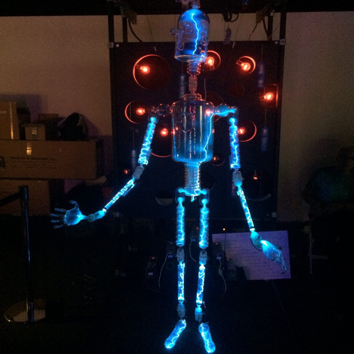
Maker Faire bills itself as “The Greatest Show (and Tell) on Earth”— a showcase of invention, creativity, and resourcefulness, celebrating Makers and Do It Yourselfers. It’s an environment where people of all ages and backgrounds gather together to share what they are making and learning. From hobbies and unique inventions to prototypes and new products coming to market, attendees have the opportunity to get up close and personal with the projects and their creators.

We at EE Journal love attending Maker Faire every year and being inspired by the energy and passion behind the engineering projects. The excited exchange of ideas and and information fills the tents at Maker Faire and we can’t get enough of it! 

And check out our previous coverage of World Maker Faire:

What World Maker Faire Shows Us About the Future of Engineering

The Maker Movement and the Spirit of Innovation

The 5 Best Things from World Maker Faire 2015

Makers Conquer the World: From Artisan to Arduino at World Maker Faire


Leave a Reply

featured blogs
Apr 25, 2024
Structures in Allegro X layout editors let you create reusable building blocks for your PCBs, saving you time and ensuring consistency. What are Structures? Structures are pre-defined groups of design objects, such as vias, connecting lines (clines), and shapes. You can combi...
Apr 25, 2024
See how the UCIe protocol creates multi-die chips by connecting chiplets from different vendors and nodes, and learn about the role of IP and specifications.The post Want to Mix and Match Dies in a Single Package? UCIe Can Get You There appeared first on Chip Design....
Apr 18, 2024
Are you ready for a revolution in robotic technology (as opposed to a robotic revolution, of course)?...

featured video

How MediaTek Optimizes SI Design with Cadence Optimality Explorer and Clarity 3D Solver

Sponsored by Cadence Design Systems

In the era of 5G/6G communication, signal integrity (SI) design considerations are important in high-speed interface design. MediaTek’s design process usually relies on human intuition, but with Cadence’s Optimality Intelligent System Explorer and Clarity 3D Solver, they’ve increased design productivity by 75X. The Optimality Explorer’s AI technology not only improves productivity, but also provides helpful insights and answers.

Learn how MediaTek uses Cadence tools in SI design

featured paper

Designing Robust 5G Power Amplifiers for the Real World

Sponsored by Keysight

Simulating 5G power amplifier (PA) designs at the component and system levels with authentic modulation and high-fidelity behavioral models increases predictability, lowers risk, and shrinks schedules. Simulation software enables multi-technology layout and multi-domain analysis, evaluating the impacts of 5G PA design choices while delivering accurate results in a single virtual workspace. This application note delves into how authentic modulation enhances predictability and performance in 5G millimeter-wave systems.

Download now to revolutionize your design process.

featured chalk talk

One Year of Synopsys Cloud: Adoption, Enhancements and Evolution
Sponsored by Synopsys
The adoption of the cloud in the design automation industry has encouraged innovation across the entire semiconductor lifecycle. In this episode of Chalk Talk, Amelia Dalton chats with Vikram Bhatia from Synopsys about how Synopsys is redefining EDA in the Cloud with the industry’s first complete browser-based EDA-as-a-Service cloud platform. They explore the benefits that this on-demand pay-per use, web-based portal can bring to your next design. 
Jul 11, 2023
32,974 views