

Moore’s Law, Moore’s Law, Moore’s Law… Up and to the right on a log scale. More of everything forever. Constantly getting bigger, faster and better; more complex, harder to design, more expensive to build, and… way, way harder to verify and debug.
Moore’s Law can make you dizzy standing still.
One thing we have learned in the past couple of decades is that prototyping complex systems before committing to silicon is basically mandatory. And programmable logic is by far the best and most widely accepted underlying technology for hardware prototyping. For most of the history of FPGA-based prototyping, the majority of companies have either built their own prototypes from scratch using off-the-shelf FPGAs on boards they develop in-house, or with ad-hoc solutions comprised of pre-made hardware from one company, design software from other companies, and the remainder of the bits and pieces scrounged together from whatever source was available.
We have reached a time when that approach probably will not continue to work well.
With the complexity of today’s systems, building a prototype can be a major design project in itself. And, keeping a high-fidelity correlation between your prototype and the thing you’re actually trying to design has become a nightmare. Inevitably your needs change as your project progresses, and the flexibility you thought you designed into your prototype board(s) isn’t enough to handle what you need to do next. And you’ll spend a considerable amount of time just debugging your prototyping board instead of making progress debugging and verifying your actual design.
Beyond that, mapping a design you created for a custom IC onto FPGA fabric is a complex process. Sure, FPGAs are programmed with RTL almost like the RTL description for your custom chip, but that “almost” is an important word. Clocking, power management, IP, multi-FPGA partitioning, and many other issues line up against you to prevent your existing RTL from working smoothly on your FPGA-based prototype.
Synopsys has long been a player in all facets of FPGA-based prototyping, and they are in a unique position of being able to offer a complete, integrated prototyping solution with flexibility probably beyond what you’ve imagined possible. The company is able to offer the prototyping hardware itself (HAPS systems), the design tools for translating and mapping your design onto the prototype hardware (courtesy of their ProtoCompiler technology), and the IP support required to put the same modules in your prototype that you are using in your actual design.
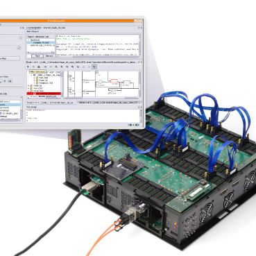
Now, the company is rolling out their latest generation prototyping system, HAPS-80, and it’s a doozy. The capacity is mind-boggling. HAPS-80 uses the formidable Xilinx Virtex UltraScale VU440 FPGAs, which pack a whopping 4.4M LUT4 equivalents per device, yielding an estimated 26 million ASIC gate capacity per FPGA. HAPS-80 has modular expansion capability allowing you to put in up to 64 of those VU440s, yielding an estimated 1.6 billion ASIC gate capacity (and putting a formidable dent in your prototyping hardware budget at the same time).
Performance-wise, HAPS-80 is capable of 300MHz system performance with a single FPGA, 100MHz performance with multiple FPGAs, and 30MHz performance with multiple FPGAs when using the company’s proprietary high-speed pin multiplexing system. That means you can typically boot an OS running on your prototype hardware in less than a minute. That’s a serious step up from previous-generation prototype performance.
Performance is only part of the picture in prototyping, however. You also need visibility and control. With HAPS-80, you can use the fourth generation of the company’s trace capture technology, “Deep Trace Debug Gen4” (which the company has thoughtfully abbreviated as “DTD4 Technology”) for real-time trace data acquisition and storage. With DTD4 (see, wasn’t that abbreviation convenient?) you can capture up to 1000 signals per FPGA in real time. The ProtoCompiler software automatically builds in debug trace memory. This lays the groundwork for almost simulator-like debugging capabilities with Synopsys Verdi.
One way a hardware prototype is different from your software simulation (apart from orders of magnitude better performance, of course) is iteration time. You don’t want to wait around for days before the prototype is ready to run again every time you make a small tweak to your design. Iteration time and bring-up time are both functions of the design software, and that’s where Synopsys has a clear advantage over the field. Because of the company’s extensive history, experience, and technology base in ASIC and FPGA synthesis, prototype partitioning, simulation, and debug, there is a wealth of capability available to apply to the problem. That capability is delivered through ProtoCompiler in particular, as well as the entire suite of prototyping tools the company delivers.
It’s not uncommon for the prototype bring-up to become a critical-path schedule item for a project, so getting your prototype up and running as quickly as possible is crucial.
Synopsys claims that you can typically bring up a prototype in less than two weeks, including partitioning your design across multiple FPGAs. That’s far, far faster than you’ll manage developing your own prototype or assembling one from a mixture of boards and tools from multiple vendors. Faster bring-up also gives you more time to use your prototype for development, debug, and verification.
Speaking of partitioning among multiple FPGAs, Synopsys offers very credible automatic partitioning technology. Most design teams shun automatic partitioning, and for good reason. Historically, automatic partitioning was a mess, and you could get better results with less effort by manually dividing your design up among multiple FPGAs. But Synopsys (and Synplicity prior to that) has been developing and marketing automatic partitioning technology for almost two decades now, and their automatic partitioning is really worth a look. Their automated pin multiplexing technology helps address one of the fundamental challenges of partitioning – lack of interconnect resources between FPGAs.
The modular architecture of HAPS and associated tools allows for a very flexible mix-and-match approach on hardware, virtual, and emulated components. You can have some modules in your prototype be the actual system hardware, others can be FPGA versions of modules that will eventually become custom hardware, and still others can be simulated virtual models. This gives you the ability to trade off visibility and control with performance on a module-by-module basis. As your design evolves, you can change the configuration to suit your project needs.
There are a lot of companies producing off-the-shelf FPGA prototyping boards. With HAPS, Synopsys has a very competitive hardware platform in its own right. But, the real differentiator in the Synopsys offering is the software and the integration of the entire prototyping platform. Because Synopsys has taken the extra effort to smoothly integrate their various components – RTL synthesis for FPGA and ASIC, partitioning, simulation, emulation, IP, and virtual prototyping technology – all collaborate to provide a highly capable prototyping platform, supported by a single company. The platform also offers capabilities you would almost certainly not find in non-integrated solutions such as remote and farm-use modes, which come in particularly handy when your prototype is being used for software development.
Synopsys says HAPS-80 and associated tools are available immediately, and hardware modules are backward compatible and interoperable with previous (HAPS-70) versions.


