


New Xilinx CEO Victor Peng made his public debut by sketching out the latest vision for the world’s leading FPGA company last week, and it included a bold claim – that Xilinx was inventing an entirely new category of semiconductor device, the Adaptive Compute Acceleration Platform (ACAP). We’ll say right up front that there is precious little information available on these future devices; the first examples of them will be based on TSMC’s upcoming 7nm process and won’t be shipping until sometime in 2019 at the very earliest. And, as one might expect, Xilinx’s “vision” pitch was more at the level of “explaining IoT infrastructure to your truck-driving Uncle Cletus from Memphis” than a “deep-dive for engineers.”
Peng first went through the usual major market drivers that we hear in just about every technology pitch these days, with zero new insight. Namely, that there is lots of data out there (and getting to be more every day), that AI will be key to doing something interesting with all that data, and that traditional von Neumann architecture machines (well, OK, he said “conventional CPUs” because, you know – your uncle) won’t cut it. The answer? Say it with me! (HINT: We’ve told you the answer MANY times, including almost four years ago when we gave it as the reason Intel should consider buying Altera.) That’s right! “FPGA-based compute acceleration!” (except Peng said “adaptable accelerated computing” because – you REALLY don’t want to get into trying to explain FPGAs to you-know-who).
OK, maybe your uncle has been really successful with that truck of his, invested his savings thoughtfully, and now he finds himself as an activist investor on the board of directors of a large semiconductor company looking to jump on the semiconductor consolidation bandwagon, and his company wants to buy themselves some smaller, more innovative semiconductor companies to “add to their portfolio, enhance shareholder value, and exploit key technological synergies.” (Hey, we said your uncle was a truck driver, not an idiot.) If you were Xilinx and you were looking to be acquired, wouldn’t you want him to feel like you were kicking it up a gear, putting the pedal to the metal, and getting ready to deliver some serious new technology that went WAY beyond boring-old FPGAs?
I certainly would.
Well, Uncle Cletus will not be disappointed, because Xilinx is loaded up and truckin’, and they’re gonna do what they said can’t be done. Peng says Xilinx has a three-part plan for the future. They are going to attack the “Data Center First” (making the cloud great again, we presume); then “Accelerate Growth in Core Markets” (i.e. continue to battle Intel/Altera for high-value FPGA sockets in areas like automotive, wireless infrastructure, wired communications, audio/video/broadcast, aerospace/defense, industrial/scientific/medical, test/measurement/emulation, and consumer); and, finally, the new crown jewels, “Drive Adaptive Computing” with what the company claims is an entirely new class of semiconductor device: “Adaptive Compute Acceleration Platforms (ACAP)”.
This is where things get both interesting and confusing.
If “Data Center First” is really Xilinx’s official new mantra, that does entirely change (for public and prospective suitor consumption at least) the priorities the company has followed for the past thirty-plus years. Until now, Xilinx’s strategy could be described as “Accelerate Growth in Core Markets First” (with basically the same ever-evolving list of key FPGA markets above) and then “Explore New Market Opportunities for Programmable Logic Technology” (i.e. find new lucrative applications for FPGAs). So “Data Center First” would imply that the company has now identified a new, highest-value, highest-growth potential market for FPGAs, and that market is… (drum roll)… the data center… Again, just like we said back in 2014.
Xilinx has been executing on a data-center vision for the past four years, securing several major wins in data-center acceleration with FPGAs, including at least a couple within the prestigious “Super 7” companies: Alphabet, Amazon, Facebook, Microsoft, Alibaba, Baidu and Tencent, who together reportedly spent around $17B in data-center capex in 2016. The rack-server market alone is forecast to pass $90B by the 2020 time frame.
Yep, sounds like a big ’ol market, alright! And it’s all Xilinx’s for the taking with practically no obstacles – except the small matters of Intel’s near monopoly on servers (accounting for 95.7% of the total servers shipped in 2016), NVidia’s dominant share of the acceleration market (selling about $2B/yr worth of GPU accelerators into data centers), and Intel’s $16.7B acquisition of Altera specifically for the purpose of competing with NVidia on that data-center acceleration play. To frame it another way, NVidia earns almost Xilinx’s entire annual revenue in GPUs for data-center acceleration alone.
OK, maybe that’s not such an easy new market to capture.
Clearly what Xilinx needs, and what this new vision seems meant to convey, is a new weapon to accelerate their participation in the current trend of explosive data-center accelerator market growth. To that end, Xilinx did what Xilinx does – they designed a new family of chips – ACAP. And, both the first and third strategic priorities now amount to using ACAP to win the data-center acceleration game. Obviously, then, this mysterious ACAP is either some new/improved data-center processor (look out, Intel!) or some new/improved accelerator meant to pair with Intel/Xeon processors (look out, NVidia and Intel PSG aka Altera).
Except – Peng said an interesting and confusing thing. He said ACAP is going after IoT from edge to data center. Weird. Those are completely different problems with massively different challenges. A little confused, there, Uncle C? We are too. It’s like saying this new piece of heavy equipment we’re selling is both a long-haul semi AND a backhoe. Yep, must be some weird lookin’ rig!
Next, Peng’s presentation veered away into… Uh, better go grab some coffee, Unc. We’re gonna talk engineering here for a bit. We’ll call you back when it’s safe.
At this point, we actually turned to some Xilinx technical experts for some conceptual clarity to fill the holes in Peng’s pitch.
So, what does ACAP look like? It looks to us like, well, the current Xilinx Zynq UltraScale+
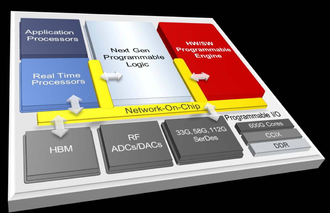
If you walk through the block diagram, you’ll see every block you’d expect in a one-generation update of Xilinx’s Zynq MPSoC, and most of them are already in the current generation:
Application Processors:
- The current Zynq has quad-core 64-bit ARM Cortex A-53s.
- ACAP will have… well, we don’t know. Probably something similar. The Xilinx experts tell us ACAP is NOT designed to push Intel/Xeon out as the core processing engine. ACAP (as the acronym implies) is an accelerator, so it will be going head-to-head with NVidia GPUs, Intel/Altera FPGA-based accelerators, and so forth.
Next-gen Programmable Logic:
- The current Zynq has up to ~275K LUTs plus a rich assortment of FPGA IP such as DSP blocks, block RAM, distributed RAM, fancy IOs – all the accoutrements of a typical FPGA.
- ACAP will have “next-gen” FPGA fabric. Probably a typical one-generation improvement.
Real-time Processors:
- The current Zynq has a dual-core ARM Cortex-R5-based real-time processing unit
- ACAP will have… something. We’re not sure. If there are “embedded” flavors of ACAP and not just “data center” versions, the real-time processors will be much more important.
HBM (Memory):
- The current Zynq has 36Mb on-chip RAM (UltraRAM) with ECC plus a rich assortment of other block and distributed RAM resources
- ACAP will have… Hey! We got one! HBM. Probably HBM2, actually, but we’re guessing here. Maybe as much as an 8GB stack. HBM3 won’t go into volume production until 2020, so unless Xilinx is WAY late with ACAP, we got some HBM2 coming.
RF DAC/ADC:
- The current Zynq RFSoC packs 8x 4GSPS 12-bit ADCs and 8x 6.4GSPS 14-bit DACs
- ACAP will apparently have something, too – we don’t know what. With all of the flavors of 5G coming, the RF front end market will become brutal. Although Xilinx’s current RFSoC offering is compelling, it’s hard to see them competing in the ACAP time frame with the vast field of companies dedicated to solving 5G RF challenges. Will we see ACAP in data centers, embedded applications, AND 5G radio heads? It slices, it dices…
SerDes:
- The current Zynq has up to 32 GTH transceivers operating at up to 16.3Gb/s
- ACAP will have… BINGO! We got another one, kinda. Last week Xilinx said their new 112 Gbps PAM4 transceivers will be part of their upcoming 7nm product line. Will that include ACAP? Probably. How many? No idea.
GPIO & Mem I/F:
- The current Zynq has… WAY too much stuff to list here. Look it up yourself.
- ACAP will have a bunch of stuff too. No mention was made of what, of course.
Network on Chip (NoC):
- Now we have arrived at the first block where something architecturally “new” could be important. Zynq UltraScale+ uses AMBA AXI4 implemented on top of what amounts to conventional bus structures. All of the Xilinx IP for Zynq UltraScale+ connects via AXI4, and there is an enormous overhead associated with that, including massive busses dominating on-chip routing and IO channels, and complex schemes for getting the chips configured and booted up and running.
- With ACAP, we are told that there is an entirely new hardware NoC routing layer, so AXI4 will be living in a true dedicated, grown up, NoC environment with separate transaction, transport, and physical layers. There are numerous advantages to this, but two are key. First, the NoC layer will eliminate the untenable congestion issues caused in the current generation by proliferation of massive busses. Second, the NoC will be functional on chip power-up, which means that ACAP will not rely on tons of LUT-based soft networking stuff to be loaded from a configuration bitstream in order for a chip to start doing actual work. However, on the downside, a chip-wide NoC will require copious amounts of interconnect, hence additional metal layers on the chip.
HW/SW Programmable Engines:
- Well, it all comes down to this. We’ve been through the entire ACAP block diagram, and the only thing that isn’t just a natural evolution of Zynq UltraScale+ is this new block. What is it? Peng says they are not ready to share details yet. We can speculate, though. We assume it is something connected to the rest of the chip via the new NoC where various payload accelerators can be dynamically loaded and swapped. Want to do neural net inferencing? Swap in that accelerator. Want to do video analytics? Swap in a different one. Again, this is just speculation on our part. Xilinx wasn’t generous with their hints.
- Further, Xilinx says that this thing is truly software programmable, meaning programmable by a software engineer using something like C with conventional compilers. This also means NOT bringing in hardware engineers, running HLS on some purpose-written hardware flavor of C, then synthesizing the resulting RTL, then running place-and-route and timing closure, then (30 or so hours later) loading a bitstream into FPGA fabric to implement the new functionality. That would make ACAP just another FPGA-based accelerator. But – what is this mysterious computing hardware? Xilinx is tight-lipped.
- Let’s take some guesses: Is it GPUs? Could be. Is it something like a conventional DSP processor? Maybe. Could it be simply more FPGA fabric set up to be quickly, dynamically loaded up with any of a library of predefined application payload accelerators? Our bet would be on this one, but when we started talking LUTs we got the impression from Xilinx we were “getting colder.” So, we’re left visualizing some kind of variation on a very-multi-core GPU/DSP-like architecture with some serious parallel datapath capability for multiplying and accumulating at numerous levels of precision.
By now, you may see what we see – ACAP is a next-generation Zynq device. Well, technically, it would be TWO generations after Zynq UltraScale+ from a process node perspective, since Xilinx is skipping 10nm and jumping straight from 16nm to 7nm. And, giving Zynq UltraScale+ a two-node jump up Moore’s Law is bound to produce some spectacular results.
ACAP should be an amazing family of chips, the likes of which the world has never seen.
But what about Peng’s claim that ACAP represents an entirely new class/category of device, and the most important since the advent of the FPGA itself? This is really a semantic argument for Xilinx to sell or fail. Xilinx claims that they invented the FPGA, so they probably assume they have the right to kill it as well. Over the decades, there has been an enormous gamut of devices that were labeled “FPGAs.” And, with each new variant, more new things were added – DSP blocks, memories, processor cores, SerDes, hardened interfaces – the list just kept growing, and the “FPGA” part just kept shrinking in importance.
But, Xilinx already tried to bag the FPGA label years ago. This is round two. When the first Zynq devices were launched, the company declared that these were NOT FPGAs. They were a new category of device, dangit – MPSoCs. (OK, they went through a few more really embarrassing attempts to name them before that, but we’ll ignore those for the moment.) Uncle Cletus may have bought that MPSoC, but engineers knew that these were really just the newest, fanciest FPGAs. Altera didn’t help, as they launched their competing devices and simply called them SoC FPGAs.
And, on the surface, ACAP looks like simply another attempt at a new label slapped preemptively on the next generation of SoC/FPGA. Why try again? Maybe, since they worked so hard to sell Zynq as an embedded processor, they needed a new term for “Zynq for Data Centers.” And that may be where the conceptual/semantic problem resides. I’m sure NVidia doesn’t love calling their data-center accelerator chips “GPUs” either, since their use has pretty much nothing to do with their origin as graphics engines for gamers.
This time, however, Xilinx argues, the device TRULY IS different. You don’t have to load a bitstream or configure any LUTs to get it running. And, bitstreams have always been the DNA marker that uniquely identified FPGAs. This, says Xilinx, means that they have finally crossed the line (for real this time) into “not an FPGA.” Seems like last time, Xilinx just wanted to convince Uncle C. Now, they want to convince us.
But, Xilinx is an FPGA company. The single reason for their three decades of leadership, the single thing that has always distinguished and defined Xilinx as a company – has been their ability to generate customer success with FPGA technology. Xilinx did this with four things: highly-skilled chip design, ultra-competent FAEs and support structure, very good design tools, and high-value IP. All four of those elements were required to make FPGAs useful. All four of those are what allowed Xilinx to crush the competition for three decades. And of those, chip design is arguably the least important. Numerous companies have challenged Xilinx with novel, innovative, and possibly “better” FPGA chip technology. All of them have failed for the same reason – because FPGAs are VERY hard to use. Xilinx killed their competitors for thirty years with their mastery of FAE support, software, and IP.
Xilinx’s strength, however, was also the FPGA market’s key weakness. The extreme challenges of FPGA use made penetrating new markets such as data-center acceleration a slow and difficult process. Xilinx couldn’t ship an army of FAEs to every place in the world wanting to use data-center acceleration. They couldn’t afford to tell software programmers that there was a 30-hour cycle time on software compiles (and by the way it involves some RTL and logic synthesis and place-and-route and there might sometimes be timing violations). FPGAs offer spectacular performance and power-efficiency advantages in computing, but with the capabilities of today’s design tools, they’re just too hard to adopt. It’s a hard sell.
So, Xilinx creates ACAP with the goal of making a data-center accelerator chip that isn’t an FPGA and therefore doesn’t require the whole FPGA support infrastructure (Xilinx’s primary core competence) for success. That means Xilinx will now be competing based mostly on their strength in chip design, without their usual competitive advantage of superior design tools, hardware IP, and customer-success FAEs. That means they are going head-to-head with highly-determined and entrenched NVidia and Intel in their own wheelhouses.
So what’s up with the vision? There are two different possibilities.
First, Xilinx may be betting the farm on a moonshot (to mix some metaphors). They may see so much potential in the data center that they are willing to risk their solid FPGA leadership to capture it. Xilinx’s technical team are certainly embarked on this journey, and they believe passionately in it.
But the second possibility is based on the preponderance of rumors around Silicon Valley that say that Xilinx is positioning themselves for acquisition, and the new management team has been brought in to put a bow on the company and dress it up for just that purpose. With the relatively flat growth curve of the FPGA market, it would be hard for Xilinx to command a premium price based only on being #1 in FPGAs. What they need is something to impress our activist investor uncle. They need to make a plausible case to him that they might be a big player in a $100B data-center market within a couple of years, rather than simply continuing to dominate the $5B FPGA market, which, in the most aggressive forecasts, will not reach $10B within the next five years.
To make this case, Xilinx doesn’t need to actually succeed in the data center, or even to convince their current engineering-savvy customers that their data-center vision is sound. Xilinx investors and executives will have already cashed out before ACAP ever ships. They just need to convince Uncle Cletus.
But, the competition in data-center acceleration will be extremely interesting to watch. So interesting, in fact, that we’ll have part 2 of this series coming up soon, when we weigh ACAP against its formidable primary competition – Intel and NVidia.


What do you think about Xilinx’s new vision and ACAP? Will they challenge NVidia’s lead in the data center acceleration market? How will it stack up against Intel/Altera’s “Falcon Mesa”? (We’ll have a follow-up article on this exact topic very soon.)
It’s nice that they are talking about the data center. It’s a huge market. Their story is “use our parts to accelerate your software” but they don’t use their parts to accelerate their own software. Until an FPGA manufacturer goes through the exercise of accelerating their own software they will never know the real pain that goes into that exercise. We will all know these guys are serious when they can tell you “buy one of our boards and we’ll place and route your software 100x faster”. I see no talk about double floating point in this ACAP (a term that died in the late 90’s after the Darpa program). I don’t see anything about a compiler that can compile a million line program and generate partial bitstreams to be swapped in and out automatically. Today if I wanted to compile a million line program for an FPGA I’d have to let the compiler run for a year. By using their own compiler for their own software they will learn what it takes to break into the data center and take it over.
It’s the right sounding words so that’s a start, but we will know they are serious about it when they use their own FPGAs to compile to an FPGA.
Right on the money BKM!
All of these heterogeneous computing “solutions” aren’t complete until they can be used in common software development environment. OpenCL and Cuda don’t count in this regard.
It can be done, but I’m skeptical that semiconductor companies can make that part happen. I think some smart person/company out there can make it happen outside of the corporate bubble. Perhaps, even a community of smart open source programmers…if given the right motivation and proper IP access? Who knows?
Interesting times, eh?
@Ura: Current tools(compilers) for chip design will have to give up constructing registers from individual dFF’s and using LUTs as if they were simple gates. Use of memory blocks as arrays of registers and for microprogram control will allow chips to actually execute if/else, for, while, do, and assignment statements.
So write the application in C or whatever, debug the code, and then parse the syntax tree to build a stack based processor runs at accelerator speed.
Here is a link that mentions the advantage of microprogram control — which by the way is just a LUT on steroids — and is great for control logic design.
https://www.eejournal.com/article/fifty-or-sixty-years-of-processor-developmentfor-this/
I am making good progress on a CEngine design that does the above