


In the relatively narrow world of FPGA-based prototyping and emulation, bigger FPGAs are always better. Always. With its 18.5 million logic cells, AMD’s Versal VP1902 Premium Adaptive SoC has just taken the “World’s Largest FPGA” title by more than doubling the capacity of AMD’s previous extra-large offering, the Virtex UltraScale+ VU19P FPGA with 8.5 million logic cells. The VP1902 SoC is also many millions of logic cells larger than any competitive programmable-logic device. Samples of the VP1902 SoC are scheduled to be available in Q3 of this year, and volume manufacturing is scheduled for the first half of 2024.
The assembly and packaging technology used to fabricate the AMD VP1902 SoC has roots in the Xilinx Virtex-7 2000T FPGA, announced in October 2011. That device, with 1,954,560 logic cells, introduced the world to chiplet-based FPGA manufacturing using a silicon interposer co-developed by Xilinx and TSMC. The 2.5D assembly and packaging technology developed for the Virtex-7 200T FPGA became a standard TSMC product offering called CoWoS (Chip on Wafer on Substrate). The original Virtex-7 2000T FPGA incorporated three FPGA fabric chiplets, which AMD prefers to call “Super Logic Regions” or SLRs, bonded to a silicon interposer. The follow-on Virtex-7 580HT FPGA replaced one of those FPGA fabric SLRs with a smaller transceiver chiplet, which allowed the device to have 28Gbps transceivers at a time when monolithic 28nm CMOS couldn’t go that fast. For both of these FPGAs, chiplets were arranged end to end along one dimension to simplify inter-chiplet wiring on the silicon interposer. The Versal VP1902 SoC incorporates four identical FPGA fabric chiplets, arranged on the interposer in a 2×2 array, as shown in Figure 1.
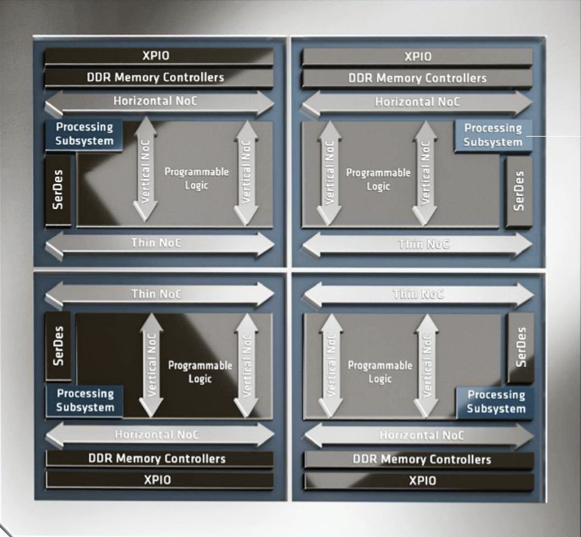
Figure 1: The AMD Versal VP1902 Premium Adaptive SoC assembles four FPGA fabric chiplets into a 2×2 array on a silicon interposer to create one packaged device with 18.5 million logic cells. Image credit: AMD
FPGA-based emulation and prototyping used for silicon and software verification before tape-out has become increasingly important as ASIC and SoC design complexity grows, because the cost of making a design error incurs significant financial costs including millions of dollars for additional mask costs and, perhaps even more important, missed market windows. Fabless semiconductor vendors, IDMs (independent device manufacturers), and systems companies are designing ever larger SoCs, so the emulation and prototyping vendors are always trying to catch up with the gate densities made possible by today’s most advanced semiconductor process technologies. Consequently, there’s always a demand for larger FPGAs to meet the resulting needs of the FPGA emulation and prototyping market. Emulation and prototyping tool vendors have proven time and again that they are willing to buy the largest FPGAs for their FPGA-based emulation and prototyping tools systems because the cost of those programmable-logic devices pales in comparison to the cost of one missed market window caused by a critical design bug.
In addition to its larger gate capacity, the AMD Versal VP1902 SoC more than doubles the available aggregate transceiver bandwidth to 12.2Tbps through 160 high-speed SerDes transceivers (32 GTM 32.75/112Gbps transceivers and 128 GTYP 32.75Gbps transceivers) compared to the Virtex UltraScale+ VU19P FPGA, which offered 5.4Tbps of aggregate transceiver bandwidth through 80 GTY 32.75Gbps transceivers. This newest Versal Premium SoC also incorporates the Versal NoC (network on chip), which AMD claims can accelerate design debug by a factor of 8 compared to the NoC-less UltraScale+ VU19P FPGA. AMD says that it also has improved the FPGA fabric’s readback mechanism in the VP1902 SoC to further enhance its debug capabilities for emulation and prototyping applications.
If you examine Figure 1 closely, you’ll see that FPGA fabric is not the only resource built into the four chiplets in the VP1902 SoC. Each chiplet also incorporates a Versal processing subsystem and multiple DDR memory controllers. This processing system is the same scalar processing system used in previous Versal devices, which includes two Arm Cortex-A72 application processors and two Arm Cortex-R5F real-time processors. The VP1902 SoC does not incorporate the Versal AI engines.
AMD is targeting the Versal VP1902 SoC at three main markets: FPGA-based emulation and enterprise prototyping, desktop prototyping, and test and measurement (T&M) equipment. FPGA-based emulation and prototyping systems appeared in the late 1980s. Pioneers in this market included IKOS Systems, Mentor Graphics, PiE Design Systems, Quickturn Design Systems, and Zycad. As part of the VP1902 SoC announcement, AMD provided a very interesting timeline that shows the evolution of FPGA-based emulation and prototyping equipment over the years, starting in 2006 and ranging from 5 million to 60 billion equivalent gates (see Figure 2 below). That’s an increase of more than four orders of magnitude in emulation capability.
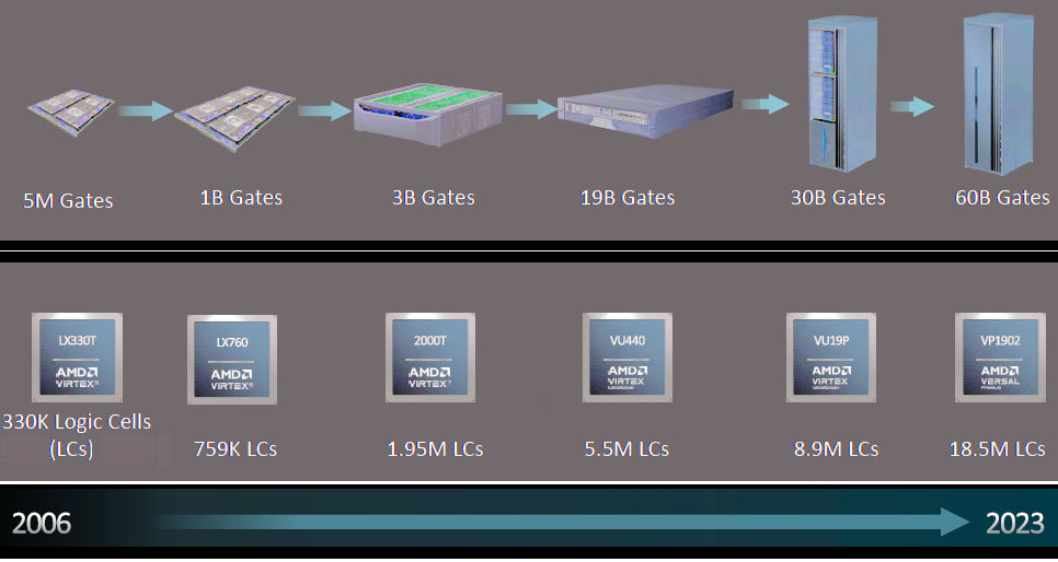
Figure 2: The capacity of FPGAs used for ASIC and SoC emulation and prototyping have grown by a factor of 56x from 2006 to 2023, allowing the capacity of systems based on these devices to grow by more than 10,000x over the same period. Image credit: AMD
Design teams developing larger ASICs and SoCs will typically use large FPGA-based emulation and enterprise-level prototyping emulators during development. Emulation equipment designed for such high-end work is networkable and can be deployed to provide 24/7 cloud access to team members distributed around the world. Smaller, lower-cost prototyping systems are used for development and debugging of IP blocks and subsystems that will subsequently be designed into ASICs and SoCs. These smaller prototyping systems also can be used to develop software and firmware for smaller IP blocks.
The T&M market is an important one for large FPGAs. T&M equipment makers must often develop test equipment before relevant standards are finalized. Consequently, test equipment makers often use programmable-logic devices to provide the flexibility needed to adapt to changes in the supported standards before the initial standard is finalized and to accommodate updates to the standard in future revisions. Equipment for testing high-speed Ethernet and wireless standards are examples in this category.
Big silicon alone will not allow FPGA-based emulation and prototyping system vendors to develop usable products. The emulation and prototyping software is equally important. AMD will be adding new features to its Vivado ML design suite to ease the incorporation of the Versal VP1902 SoC into these systems. The new software features in Vivado ML support more efficient hardware development using the VP1902 SoC and include automated design closure assistance, interactive design tuning, remote multi-user real-time debugging, and enhanced back-end compilation, which allows end users to iterate their IC designs more quickly. AMD expects that these features will appear in a Vivado ML release later this year.
In addition, tools from the major EDA vendors must also be adapted to the Versal VP1902 for the device to work effectively when used in emulation and prototyping systems. In its announcement for the VP1902 SoC, AMD says it’s collaborating with EDA vendors including Cadence, Siemens, and Synopsys to develop an EDA ecosystem for emulation and prototyping work. AMD’s Vivado ML will continue to act as the intermediary between the EDA tools from these vendors and the silicon.
These large programmable-logic devices, from any vendor, are the most expensive devices that FPGA makers manufacture because they always push the envelope of what’s possible at any point in the industry’s evolution of Moore’s Law. AMD’s use of chiplets (or SLRs) to create the VP1902 SoC is a reticle-busting approach to FPGA construction, which allows the creation of a programmable-logic device that’s much larger than any achievable monolithic IC. Although it prefers to use the word “tiles” rather than “chiplets,” Intel also employed chiplets when creating the Stratix 10 GX 10M, with 10.2 million logic elements. The Stratix 10 GX 10M FPGA, introduced in late 2019, held the “World’s Largest FPGA” crown for about 3.5 years. (See “Intel’s “World’s Largest” FPGA.”) In fact, Intel has used chiplets extensively in its Stratix 10 and Agilex FPGA families for several years.
One disadvantage of chiplet-based construction for FPGAs appears at the die-to-die interface. Connections are costly at that point and the inter-die interconnect density is lower, so there are fewer interconnects per millimeter of beachfront between chiplets compared to the interconnect density within the on-chip FPGA fabric. In addition, die-to-die interconnect is generally slower than on-die interconnect. Consequently, the use of multiple chiplets creates I/O bottlenecks. As Figure 1 suggests, there was no way to weave the independent FPGA fabrics on the four chiplets in the VP1902 SoC together into one seamless programmable-logic fabric, so there’s a discontinuity as signals in the fabric traverse the die-to-die interconnect. It may well be that AMD uses the NoC to interconnect the four FPGA fabrics in the VP1902 SoC. In any case, the vendor’s design tools usually attempt to minimize this discontinuity as much as possible through careful block placement, so that only lower-speed buses traverse these die-to-die interconnect bridges. AMD has stated that it is enhancing the place-and-route and partitioning capabilities of its Vivado ML tool suite to accommodate multi-tile devices like the VP1902 SoC.
Intel and AMD regularly pass the “World’s Largest FPGA” title back and forth, and the industry benefits from the competition. AMD’s Versal VP1902 SoC has now raised the bar for the world’s-largest title by about 80% over the previous title holder: the Intel Stratix 10 GX 10M. However, Stratix 10 FPGAs are not the newest programmable-logic critters in Intel’s stable. The newest Intel FPGA family is the Agilex FPGA and SoC product line, which Intel has been rapidly expanding, so it’s probably only a matter of time before Intel retakes the title by announcing the World’s Largest FPGA with a programmable-logic device based on Agilex lineage. We’ll need to wait and see if and when that happens. For now, AMD holds the title and wears the crown.


One thought on “With 18.5 million logic cells, AMD’s Versal VP1902 Premium Adaptive SoC becomes “World’s Largest FPGA””