Xilinx has been performing a slow reveal of its new ACAP (adaptive compute acceleration platform) architecture for many months, and the company unveiled much more—including the new “Versal” family name and six (!) new, multi-member series (aka families) of 7nm ACAP devices—at its October 1 Xilinx Developers Forum (XDF), held in San Jose, California. (The company says that “Versal” is a contraction of the words “versatile” and ”universal.”) In his XDF keynote introducing the Versal product lines, Xilinx President and CEO Victor Peng declared that “Xilinx is not an FPGA company; Xilinx is a platform company,” and he emphasized that Xilinx was focused on “whole application acceleration.” In fact, this is the new Xilinx mantra.
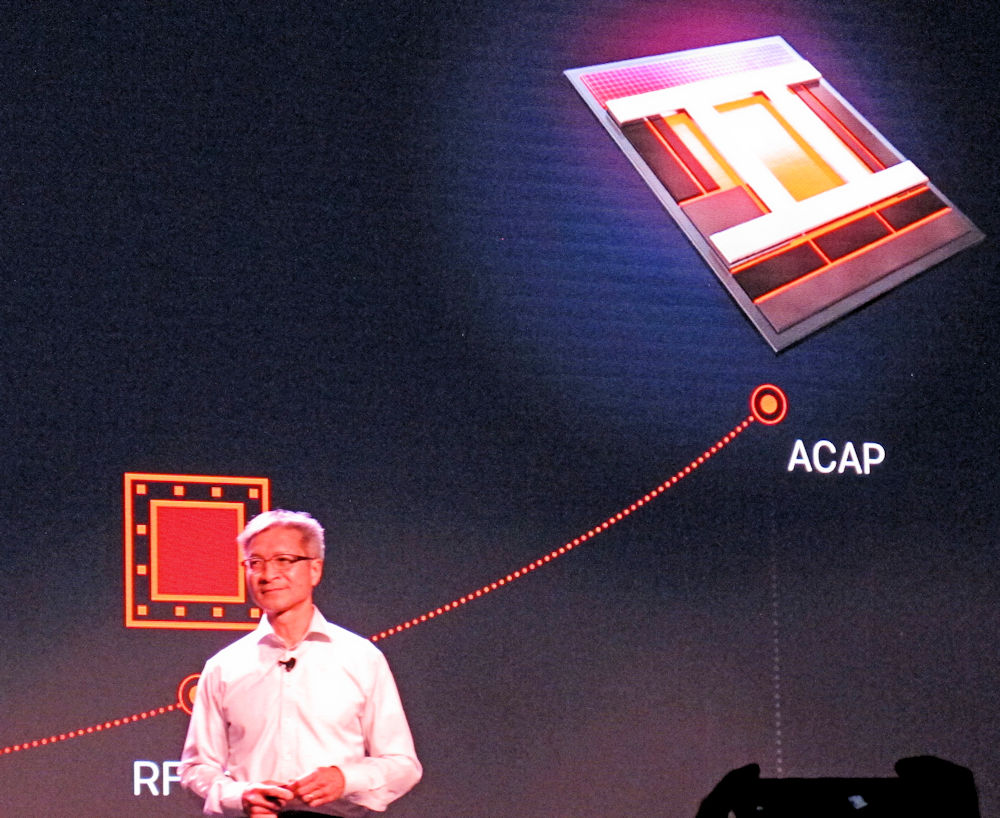
Figure 1: Xilinx’s President and CEO Victor Peng announces the 7nm Versal ACAP at last week’s XDF. (Image source: Steve Leibson)
Peng has a valid point with respect to the Versal ACAP not being an FPGA. We all recognize that a microcontroller is not a memory or a Flash EPROM, even if the microcontroller’s on-chip memory consumes most of the chip’s die area. Similarly, Xilinx insists that ACAPs are not FPGAs, although all Xilinx ACAPs contain the company’s signature FPGA array fabric (now rebranded as “Adaptable Engines” in ACAP block diagrams).
“That’s our DNA,” said Peng, referring to FPGAs.
In addition to FPGA fabric, Versal devices incorporate many other important system elements including:
-
- Scalar Engines: Arm Cortex-72 and Cortex R5 processors. These scalar engines were formerly known as the PS (Processing System) in earlier Xilinx Zynq devices and that term shows up in some Versal ACAP documentation as well.
- Intelligent Engines: AI Engines (a massive number—hundreds—of purpose-built, networked, software-programmable, VLIW, SIMD processors intended for AI processing and DSP) and DSP Engines (formerly known as DSP slices), now enhanced with hardened, floating-point extensions. Use of “engine” to describe a DSP slice sort of stretches the definition of “engine” in my book.
- Many hardened protocol blocks for a variety of standard interface and memory protocols including Ethernet, PCIe, CCIX (a chip-to-chip coherent serial protocol), and SDRAM controllers.\
- High-speed SerDes ports from 32 Gbps to 112G PAM4, and programmable I/O.
- A ton of on-chip memory distributed all over the device as local RAM for the scalar and AI engines, plus LUT RAM, Block RAM, and UltraRAM in the FPGA fabric.
- A pervasive NoC (network on chip) tying all of the engines to the many, many on-chip memories with a high-speed, multi-lane, time-division-multiplexed, on-chip, packet-based network.
- A software-controlled Platform Management Controller (PMC) that supervises booting, configuration, dynamic reconfiguration, encryption, authentication, power management, and system monitoring for the entire device. The PMC reportedly speeds dynamic device reconfiguration by 8x compared to previous-generation Xilinx devices. (Note: You won’t find the PMC on the block diagram below. It’s an entire software-programmable processor hidden in the PCIe/CCIX block located in the lower left corner. Complex devices like the Xilinx Versal ACAPs often have many such hidden processors.)
Here’s Xilinx’s conceptual block diagram of the Versal ACAP:

Figure 2: Versal ACAP Conceptual, Composite Block Diagram (Image Source: Xilinx)
Figure 2 shows a composite block diagram of all the available blocks in the Versal architecture. However, each ACAP device includes only a subset of the components appearing in the above diagram. For example, only some, yet-to-be-announced Versal devices will incorporate 3D HBM (high-bandwidth memory) DRAM stacks or 112Gbps, PAM4 SerDes ports. Surprisingly, many Versal devices will have no AI Engines at all.
To set a foundation for all of this programmable goodness, let’s start with the six announced Versal series. There are three multi-member Versal AI series, which incorporate AI Engines:
-
-
- Versal AI Edge
- Versal AI Core
- Versal AI RF
-
And three non-AI, multi-member series of Versal devices, which do not include AI Engines:
-
-
-
- Versal Prime
- Versal Premium
- Versal HBM
-
-
Of these, Xilinx provided details for five devices in the Versal AI Core series and nine devices in the Versal Prime series at XDF. That’s fourteen different devices in just the first two of the six planned Versal device series. Devices in the other four Versal ACAP device series are future parts, to be detailed later.
The six Versal device series are designed to cover what Xilinx calls mid-range and high-end applications. Understandably, there are no planned low-end 7nm devices. That’s because all 7nm devices are inherently expensive to manufacture because they’re based on FinFETs and, soon, EUV patterning (coming to a fab near you, if you live in Taiwan). In the words of Liam Madden, Xilinx’s EVP of Hardware and Systems Product Development, these 7nm devices are “wicked expensive.”
Based on the presence of three non-AI series, it’s clear that Xilinx isn’t aiming its Versal ACAPs exclusively at AI acceleration because, as the company emphasized at XDF, AI tasks like inference are just a piece of the overall end-product puzzle. AI is the new, buzz-worthy, not-so-secret ingredient that is being hot-glued to a bushel basket full of embedded applications to make them somehow “better” (and to get more money from venture capitalists).
However, from Xilinx’s perspective, it’s not sufficient to accelerate just the AI portion of the job. Real performance improvement comes from accelerating as many tasks as possible. Sample target tasks for acceleration by the AI Engines, the DSP Engines, or the Adaptive Engines (or combinations of the three) mentioned during the XDF presentations included beamforming for radar 5G wireless communications, network packet communications, and smart controllers for large solid-state storage systems in data centers.
Chock Full O’ Engines
That’s why Xilinx filled Versal devices to the brim with engines. Chances are that one of those engines will be best suited for any given task, whether you need raw performance, power efficiency, or some combination of both.
Some of the Versal’s engines need little explanation because they’re evolutionary extensions of existing processing resources found on earlier Xilinx devices. For example, the Versal ACAP’s Scalar Engines include 64-bit Arm Cortex-A72 application processors and 32-bit Arm Cortex-R5 real-time processors, which are a natural progression from the two 64-bit, Arm Cortex-A53 applications processors and two 32-bit, Arm Cortex-R processors found in Xilinx’s 16nm Zynq UltraScale+ MPSoCs. As with the Xilinx Zynq UltraScale+ MPSoCs, the Versal’s two Arm Cortex-R5 processors can run in lockstep for safety-critical applications.
Xilinx did not publicly disclose the clock rates for the Arm processors in the Versal ACAPs, but the preliminary, online data sheets do give DMIPS ratings for each Arm processor: 15,980 DMIPS for the Arm Cortex-A72 processors and 2505 DMIPS for the Arm Cortex-R5 processors. Now, VAX DMIPS/MHz ratings are no longer especially useful as workload numbers, but we can use them to back-calculate clock rates for the processors. Given the DMIPS/MHz ratings of 4.7 for the Arm Cortex-A72 processor and 1.67 for the Arm Cortex-R5 processor, thoughtfully published on the Arm Microarchitecture Wikipedia page, Xilinx’s published DMIPS/MHz numbers suggest that the company expects the Versal ACAP’s Arm Cortex-A72 processors will run at 3.4GHz and the Arm Cortex-R5 processors will run at 1.5GHz. We’ll likely know more when Xilinx has Versal silicon in hand.
All currently announced Versal ACAPs have two of each of these Arm application and real-time processors, but Xilinx presenters at XDF made it clear that the company is not constrained to using these particular Arm processors. In addition, Xilinx is not necessarily limiting future Versal ACAP designs to two application processors and two real-time processors.
The Versal ACAP’s Adaptable Engines section consists of the familiar Xilinx FPGA fabric, woven with the traditional FPGA threads of programmable logic, several forms of embedded SRAM, programmable interconnect, and DSP slices. The DSP slices, now called DSP58 slices instead of DSP48 slices (“They’re ten better than DSP48s,” quipped Madden at a post-keynote press conference), have been “significantly upgraded.” The fullest explanation of “significant” in this context appears to be that DSP58 slices now have hardened support for floating-point operations.
Although they’re physically located in the Xilinx-red FPGA fabric, the DSP58 slices also form the foundation for the green DSP Engines block shown in the block diagram above. Depending on the Versal device selected, you can build several thousand of these DSP Engines using DSP58 slices and the immediately surrounding FPGA fabric.
A Deeper Dive Into the AI Engine
The AI Engine and the NoC are the most novel parts of the Versal architecture. Although Xilinx discussed the AI Engine at length in a paper presented earlier this year at the Hot Chips 30 conference (see “Xilinx Puts a Feather in its ACAP”), Xilinx provided significantly more architectural information at XDF. The Versal AI Engine is a tiled array of hardened SIMD processors that combine 6-way instruction parallelism built into a 128-bit instruction word with 512-bit, fixed-point and floating-point vector execution units and a 32-bit scalar processor, as shown in Figure 3.
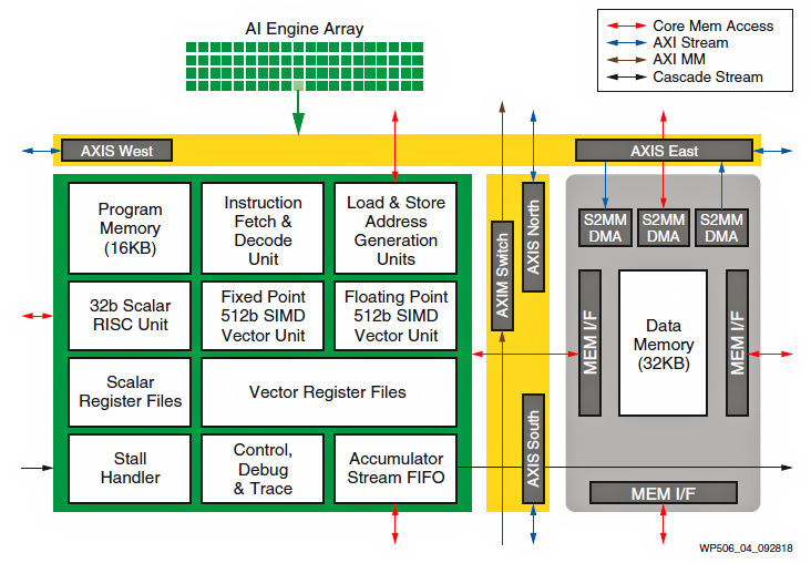
Figure 3: Each tile in the Versal AI Engine array is a hardened, VLIW, SIMD processor. (Image Source: Xilinx)
Each AI Engine tile has a 32Kbyte local data SRAM that’s also directly connected to the SRAMs in the four immediately surrounding AI engine tiles (north, south, east, and west). An AI Engine tile can “borrow” memory from these four adjacent tiles, easing the development of asymmetrical task engines.
In addition, each AI Engine tile is connected to all of the other AI Engine tiles in the array over a dedicated, streamlined NoC. Xilinx developed this lightweight NoC in house for the AI Engine’s specific requirements. It’s based on Arm’s AXI Stream protocol. A trio of DMA engines in each tile can pass data to other tiles in the AI Engine array, as shown in Figure 4, which is taken from the Xilinx presentation at this year’s Hot Chips 30 conference.
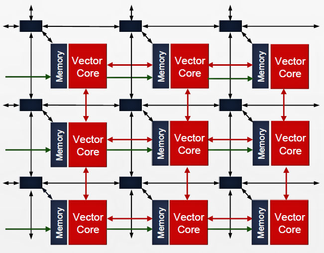
Figure 4: Each tile in the Versal ACAP’s AI Engine connects to all of the other AI Engine tiles over a dedicated, streamlined NoC. (Image Source: Xilinx)
Now, Figure 4 might cause you to seriously underestimate the processing power of the Versal ACAP’s AI Engine block because it shows just nine AI Engine tiles. You might be led to think that’s the number of tiles in an AI Engine. Actually, the smallest announced Versal ACAP in the AI Core series, the VC1352, incorporates 128 AI Engine tiles, and can execute 11 to 43 peak TOPS for INT8 and INT16 operations, or 3 TFLOPS for FP32 operations. The largest device in the series, the VC1902, has 400 AI Engine tiles, and can execute 33 to 133 peak TOPS (for INT8 and INT16 operations), or 8 TFLOPS for FP32 operations. So there’s considerably more processing power available in the AI Engine than is suggested by Figure 4.
(Note that Xilinx did not publicly disclose the clock rate for the AI Engine tile processors during XDF and there’s no way to back fit clock rates from the TOPS and TFLOPS performance ratings as I did for the Arm processors because the AI Engine tiles are an all new, Xilinx-proprietary, VLIW processor architecture.)
Instead of using the all-new AI Engine, why not just build execution hardware for AI functions such as CNNs directly in programmable logic? Of course, you can. You can already do that with existing Xilinx devices, and such implementations can be as fast as, or perhaps a bit faster than GPUs, and an order of magnitude faster (or more) than CPUs for AI inference tasks like GoogLeNet.
But the massively parallel Versal AI Engine is faster still—perhaps 2.5x faster than a GPU and 72x faster than a CPU—based on information that Xilinx provided during XDF. That’s a throughput rating for batched data. Throw in a low-latency requirement (like 2 milliseconds) for real-time applications like autonomous driving and the AI Engine’s advantage increases to 8x over a GPU, while the CPU drops out of the race entirely because it cannot meet the requirement. (Again, these are Xilinx’s numbers.)
All of this processing speed requires high-throughput, non-blocking data movement between the on-chip engines and memory. That’s why Xilinx built an additional NoC into the overall Versal ACAP architecture. A chip layout diagram (as opposed to the conceptual block diagram in Figure 1) that shows how the NoC ties the various elements of the Versal ACAP architecture together appears in the Xilinx Versal White Paper (WP506) and is reproduced in Figure 5 below.
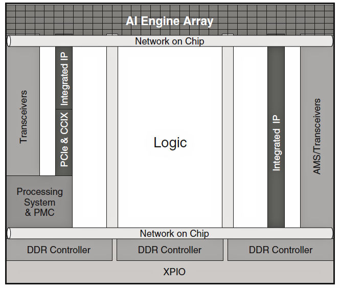
Figure 5: The NoC ties all of the Versal engines together and connects them to the many distributed on-chip memories, to the SDRAM controllers, and to the I/O ports. (Image source: Xilinx)
As Figure 5 shows, the chip-wide NoC connects all of the on-chip Versal engines together and to the many memories distributed across the devices. The chip-wide NoC provides a fast, deterministic way to move data from engine, to memory, to engine across the chip. In addition, this larger NoC connects all of these engines to the chip’s SDRAM controllers for off-chip storage and will also connect the engines to the HBM DRAM when the Versal HBM series devices become available in the future. (See the roadmap, below.)
Software is Key to Harnessing the Versal’s Engines
In his portion of the Versal rollout, Xilinx’s EVP of Software and IP Products Salil Raje said that his software-development team’s goal was to provide “a natural onramp” to Xilinx devices for developers at all abstraction levels. He then emphasized that the utility inherent in the Versal’s collection of programmable engines can be unlocked only with a huge software investment, as illustrated by the breadth of tools listed in Figure 6.
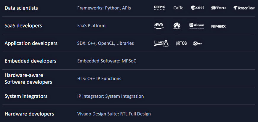
Figure 6: The amount of software required to provide programmers with familiar development tools at all abstraction levels is immense. (Image Source: Xilinx)
Data scientists are accustomed to working with frameworks such as Caffe and TensorFlow. Application developers use HLLs such as C++ or other specialized frameworks such as OpenCL. Embedded developers are accustomed to writing microprocessor code in C or C++, and they want to run that code on standard operating systems such as Linux. Wizened FPGA hardware developers know how to get the most performance out of Xilinx devices by writing RTL code using Verilog and VHDL, and they will want to continue doing so with Versal devices.
Based on Figure 6, the span of development tools that Raje’s team is tackling is immense. And yet, if Xilinx wants to welcome all comers to the Versal tent, significant support for all of these tools is a bedrock requirement. Xilinx has been writing and acquiring these tools for years. Some of these development tools were put in place with the advent of Xilinx’s 28nm FPGAs. Others were added to support the company’s Zynq, UltraScale, and UltraScale+ devices.
When asked what his team had done specifically for the Versal generation, Raje said that all of the existing Xilinx development tools had been “up-leveled” for the Versal AI Engine and that SDSoC and SDAccel, the Xilinx development environments tailored for the embedded and network worlds, had been blended together to span a broader range of applications. In addition, the software-development teams at Xilinx have been busy adding libraries for more applications. The company is now very focused on open software as well, added Raje.
Xilinx’s Versal Roadmap Stretches to 2021
In an unusual move for the company, Xilinx has laid out a multi-year roadmap for the Versal series. Devices in the first two announced series, Versal AI Core and Versal Prime, will start to ship in the second half of 2019—possibly as much as a year from now or more. Two more AI members, Versal AI Edge and Versal AI RF with integrated RF ADCs and DACs, will ship in 2020, as will members of the high-end AI Premium series with the really high-speed Ethernet IP and the 112G PAM4 SerDes ports. Finally, the Versal devices with integrated HBM DRAM will ship in 2021.
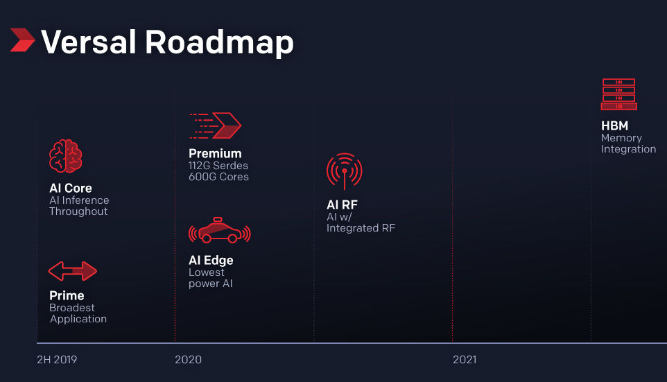
Figure 7: The Versal roadmap shows that the first two device series become available in the second half of 2019, with the other four series following in 2020 and 2021. (Image Source: Xilinx)
So, in the end, Victor Peng wants you to know that Xilinx is no longer “just” an FPGA company. It’s a platform company and it plans to support developers as a platform company should, with a big, comprehensive software toolbox that serves developers at all abstraction levels. Given a look at the Versal ACAP architecture and the company’s development-tool aspirations during last week’s XDF, it’s very clear that Peng’s sights are set many miles above the FPGA plane.
Do you think that the Versal ACAP will take Xilinx to new heights? Please leave your thoughts in the comments below.


3 thoughts on “Why does Xilinx say That its New 7nm Versal “ACAP” isn’t an FPGA?”