


“Simplify and add lightness.” – Colin Chapman
If you don’t write assembly-language programs, you’ll miss out on some strange, interesting, wonderful, or uniquely powerful instructions lurking inside your processor. Some are immensely helpful. Others are just… weird.
Any processor can add and subtract, and most can multiply integers. A few can even do integer division. And some have a floating-point unit (FPU) for dealing with fractions.
But can your chip do 4-dimensional transforms? Table lookups? Nursery rhymes?
Take the case of the Motorola 68K processor family’s TBL instruction. The mnemonic stands for “table lookup and interpolate,” and it’s remarkably powerful for such an old 1980s-era CPU design. The syntax goes like this: TBL [address], [register]. Pretty basic, right?
Here’s what happens. The address is a pointer to the start of a table of values with up to 256 entries. The data register is an index into that table. In other words, if the register holds the value 55, you’re pointing into the 55th entry in the table.
But here’s the thing. The table can be arbitrarily complex, like plotting the coordinates of a Fourier transform, or square root values, or samples from an arbitrary waveform. Completely nonlinear, in other words. What the TBL instruction does is to split your index pointer in half and use half as an index (0–255) into the table and the other half as a fractional offset between that table entry and its nearest neighbor. That is, the processor interpolates what the value between those two points would be, even though you’ve never defined it anywhere. Here’s what the actual function looks like:
Y = {(F(n+1) – Fn) x (Dx)[7:0] / 256} + Fn
Remember, this is one instruction – a built-in, hardwired, assembly-level operation. It’s not a C function call or a compiler intrinsic. The chip interpolates the correct value in between two given values, all in hardware. It uses just two bytes of code space and needs 30–40 clock cycles to execute. That’s faster than integer division. You even get to decide whether the interpolated results will be rounded or not, and whether the values are signed or unsigned.
This is a really handy function for estimating square roots without actually calculating them. It’s also good for motor control, kinematics, and processing analog waveforms. Not bad for a single instruction.
Then there’s Hitachi’s SH-4 processor, which can do whizzy 4D math all day long. SH-4 is part of the SuperH processor family, which has been around for a while and is used in all sorts of automotive and embedded systems. SuperH hit the big time when Sega chose it for its Saturn and Dreamcast videogame consoles. And therein lies the basis for the remarkable FTRV instruction.
FTRV (for floating-point transpose vector) takes a 4×4 array of floating-point numbers and multiplies each element against a 4-element vector of floating-point numbers, resulting in an array of new values. Here’s how the Hitachi manual explains it:
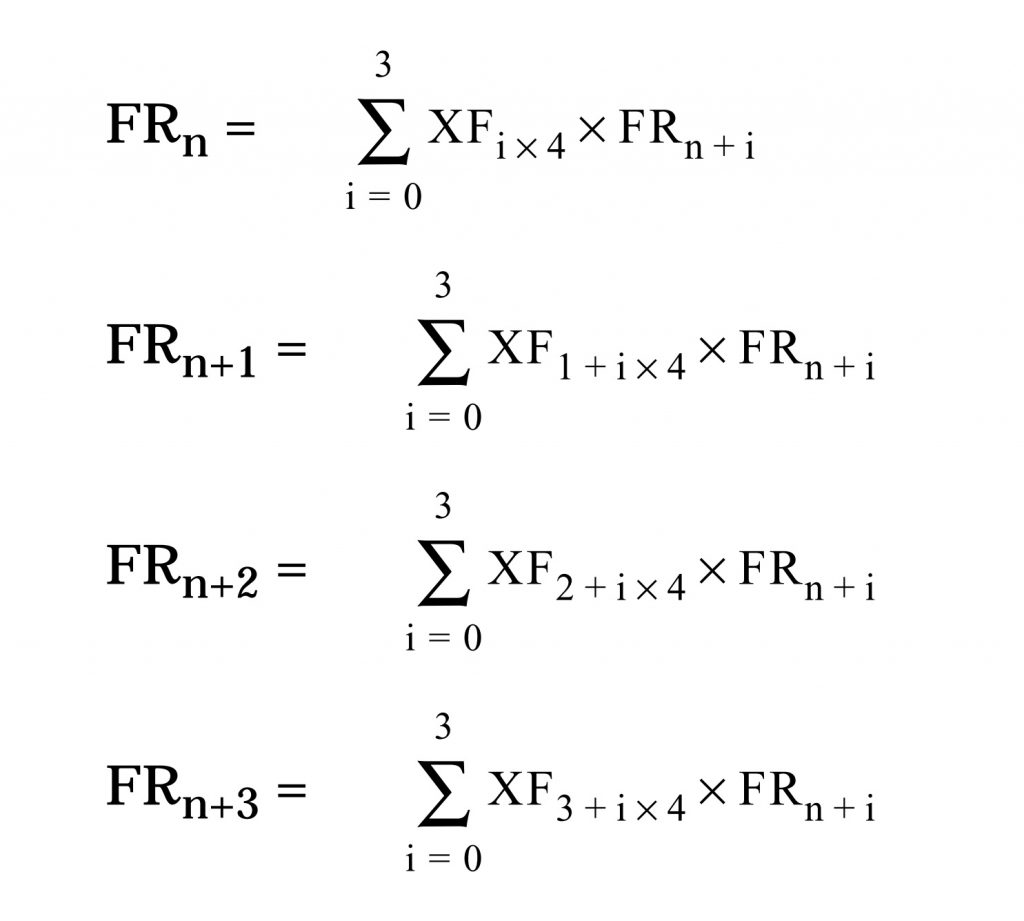
Oh, and it does all this in one clock cycle. With a single 16-bit opcode.
Why in the world would you need this? This is a dot-product, one of the basic functions of 3D rendering for video games, hence its special inclusion in the processor for Sega’s Dreamcast. You use it to calculate the angle at which a ray of light bounces off a polygon in 3D space. Pretty hard to accomplish that any other way.
Then there’s everybody’s favorite CPU mnemonic, the EIEIO instruction. It’s a PowerPC function that stands for “enforce in-order execution of input/output,” and it’s there to help out with cache coherence in high-performance systems. As such, it’s similar to other processors’ synchronization functions, but more fun. Old MacDonald had a server farm…
The same company also gifted the Power9 processor with the DARN instruction (deliver a random number). Who says IBM is stuffy?
The old DEC PDP-10 mainframe had the somewhat forced TRON instruction (Test Right, set to Ones and skip if Not- zero).
Intel and AMD used to include x86 instructions for handling BCD (binary-coded decimal) arithmetic, a number format only slightly newer than Roman numerals. The BCD-related instructions all got dropped years ago, but you used to be able to convert between binary and BCD using AAA, AAS, and AAM (ASCII adjust after addition, subtraction, and multiplication, respectively), and AAD (ASCII adjust before division). Helpful if you’re programming Nixie tubes, I guess.
I’ve worked on plenty of chips that implemented the secret HCF (halt and catch fire) instruction, although it never seemed to be documented properly.
There are lots of other examples, so feel free to contribute your favorites. But it’s oddball instructions like these that eventually led to the development of RISC – namely, reducing the instruction set.
Superpower instructions like TBL and FTRV are rarely (if ever) exploited by compilers. They simply don’t map well onto a C compiler’s view of the world, so they effectively disappear from the chip’s instruction set unless you dive into assembly language. Plus, complicated instructions like these take up a lot of hardware – hardware that’s sometimes in the critical path of the processor’s pipeline and that limits its clock speed.
So, the thinking goes, if most people are using compilers anyway, why even include such instructions? Leave ’em out and you simplify the hardware, save a few thousand gates, and maybe even remove a performance bottleneck or two. The chip might run faster, and C programmers will never know the difference.
Maybe so, but those instructions are there for a reason. They’re not just gratuitous complexity for the sake of wasting gates. They perform a useful function, and they do so far faster and more efficiently than software could. Software is very power-inefficient. Sega and Hitachi knew exactly what they were doing with their elaborate matrix geometry transforms.
I give it a couple of years before these features start creeping back into the next generation of “RISC” processors that need specialized high-value functions.


