


I have some news that will make chip and chiplet designers (we’re talking ASIC, ASSP, SoC, and multi-die systems) squeal in delight. However, before we leap headfirst into the fray with gusto and abandon (and, it goes without saying, but I’ll say it anyway, aplomb), I just got off a call with my old chum, Adam Taylor.
As you may recall from an earlier column, Adam will be hosting the inaugural FPGA Horizons US East 2026 Conference and Exhibition, April 29-30, 2026. This auspicious event will be collocated with the PCB EAST 2026 Conference and Exhibition at the DCU Convention Center, 50 Foster Street, Worcester, MA 01608.
Adam was telling me that the FPGA Horizons portion of this dual-conference combo has exceeded all expectations, to the extent that it’s almost sold out. Having said this, it’s still possible to get an FPGA Horizons 1-Day Conference pass for only $150.00. This is for Wednesday, April 29 only, and it includes all the FPGA Horizons technical sessions on that day, access to the proceedings, access to the exhibits, and access to the PCB East reception on Wednesday evening.
And now, back to the main thrust of this column. This is going to be a bit of a wild ride, so I trust you’re dressed appropriately.
I think it’s fair to say that my primary interests are science and technology. I have little truck with the business side of things (which may explain why I have so little money). When a press release crosses my desk saying that some company has just closed a new round of funding, they’re lucky if I manage to raise a quizzical eyebrow and rouse myself to say “Meh!”
I’m also less than enthused to find my inbox bulging with pseudo-news items along the lines of “The guys and gals at ParadigmShift Technologies are on the verge of engaging in a carefully considered, forward-thinking, strategically harmonized understanding with the chaps and chapesses at FutureWave Concepts to explore the feasibility of potentially initiating a loosely defined, synergy-driven, cross-domain, pre partnership dialogue regarding a possibly game-changing, next-wave opportunity that might, at some suitably vague juncture in the future, reshape the broader ecosystem in ways yet to be determined—powered, naturally, by world-class vision and stakeholder engagement.”
The bottom line is that you will rarely find me telling you things like “Company A and Company B have announced a partnership to…” Of course, this makes it all the more impactful when I do tell you that Breker Verification Systems and Moores Lab AI recently announced a partnership to create an AI-powered SoC verification flow that integrates Breker’s Trek Test Suite Synthesis with Moores Lab AI’s agentic AI technology.
The reason I’m so enthused by this is that I was just chatting with David Kelf, CEO of Breker, and Shelly Henry, CEO and Co-Founder of Moores Lab AI . Since I commenced my career designing ASICs in the days before meaningful Electronic Design Automation (EDA) tools existed—before the “EDA” term was even coined, in fact—the news imparted by David and Shelly was music to my ears.
First, let’s take a step back and remind ourselves what these companies do. Breker is one of the established players in the functional verification space, focusing on what’s often called “scenario-based verification.” In simple terms, they generate intelligent, high-level test scenarios—based on the system’s intended behavior—and automatically map them into executable test content across simulation, emulation, and silicon.
Breker’s core technology centers around synthesizing test sequences from formal models of system intent. Rather than hand-crafting endless directed tests or relying purely on constrained-random approaches, their tools create coordinated, system-level scenarios that exercise complex interactions, particularly useful for things like cache coherency, multi-core interactions, and heterogeneous SoCs.
The result is broader coverage with fewer tests, better alignment with real-world use cases, and a more scalable way to verify increasingly complex systems. As you may recall, we’ve crossed paths with these folks before—I wrote about them back in 2022 in my column Verifying Cache and System Coherency in 21st Century Systems, where their technology was already tackling the thorny problem of coherency verification in modern multi-processor designs. In short, they’ve been pushing “smarter verification” for a while now—well before AI became the latest technology du jour.
Moores Lab AI is a much newer entrant, but although it was only founded in 2025, it is already making a splash with a distinctly modern take: agentic AI for chip design and verification.
Their flagship platform, VerifAgent, is designed to automate large chunks of the verification workflow—from generating test plans and UVM testbenches to creating assertions, coverage models, and even debugging multi-file issues. The key idea is not just AI as a helper, but AI as an active participant—an “agent” that can plan, generate, execute, and refine verification tasks.
According to their corporate fact sheet, the goal is ambitious: reduce verification effort by up to 85% and accelerate silicon schedules by as much as 7X, all while integrating with existing EDA tools and flows rather than replacing them.
They’re also tackling a very real pain point. Today’s verification flows are still highly manual, fragmented across tools, and can take 6–12 months, often dominating the overall chip development schedule. Moores Lab AI’s pitch is that agentic AI can collapse much of that effort into an automated, end-to-end pipeline (the eye-catching numbers in this column’s title—10X faster and 50% lower cost—come straight from Moores Lab AI’s own fact sheet).
There’s one final topic we need to discuss to finish setting the scene: the Portable Test and Stimulus Standard, or PSS for short. Developed under the auspices of Accellera, PSS was introduced with the laudable goal of raising the level of abstraction in verification. The idea was deceptively simple: describe system-level behavior once—using a portable, high-level model—and then automatically generate tests for different targets, including simulation, emulation, and even post-silicon validation.
On paper, this was brilliant. Instead of writing separate tests for each stage of the flow, you could capture intent in a single place and let your tools do the heavy lifting. PSS promised better reuse, broader coverage, and a way to exercise complex, end-to-end scenarios that are notoriously difficult to hit with traditional approaches.
A few years ago, PSS was the darling of the verification world. People spoke of it in hushed, reverential tones. It was going to revolutionize everything. And then… it didn’t.
PSS didn’t so much fail as quietly drift into the background. Accellera is still shepherding the standard, and there are certainly pockets of adoption, but the groundswell of enthusiasm has ebbed. Some of the original architects have moved on, and for many teams, PSS ended up in that uncomfortable category of “great idea… maybe next project.”
What happened? In a word: “effort.” PSS shines when you have rich models of your IP blocks and subsystems that can be stitched together into system-level scenarios. But those models don’t create themselves. Someone needs to write them. And not just one or two, but potentially dozens, covering everything from DDR controllers to PCIe interfaces to custom accelerators.
The problem is that very few people want to learn the PSS language or write the models. The SoC team doesn’t have time. The IP teams don’t see it as their responsibility. Everyone agrees it’s valuable… but nobody wants to be the one holding the shovel.
As a result, PSS has ended up in a kind of no-man’s land where it’s admired in principle but avoided in practice. This is a shame, because the underlying idea is still incredibly powerful. The ability to describe system intent once and generate meaningful, coordinated tests across the entire lifecycle—from IP to SoC to post-silicon—is exactly what modern verification needs.
I can almost hear you thinking, “If only there were some way to automatically generate the PSS models.” Well, it’s funny you should say that…
What Breker and Moores Lab AI bring to the table is, quite literally, a marriage made in heaven. On the one hand, we have Moores Lab AI’s agentic AI, which can ingest specifications—architecture documents, design descriptions, programming models, and so forth—and automatically generate the artifacts that engineers are traditionally obliged to create by hand.
We’re not just talking about high-level summaries or vague suggestions. This AI can take those specs and turn them into concrete verification assets: test plans, UVM testbenches, assertions, coverage models, and—crucially for our discussion—PSS models. In effect, it transforms raw design intent into an executable verification representation.
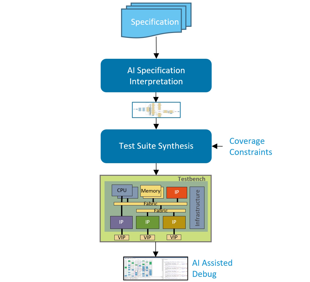
The combined Breker + Moores Lab AI flow (Source: Breker and Moores Lab AI)
On the other hand, we have Breker’s mature back-end technology, which has spent years learning how to take those high-level models and synthesize them into coordinated, system-level test scenarios. Their tools know how to map intent into tests that run across simulation, emulation, and silicon, while handling the messy real-world details—debug, coverage closure, and platform integration.
Individually, each of these capabilities is impressive; together, they’re transformative. Moores Lab AI provides the missing front end—the ability to take a specification and automatically create the models that no one wants to write. Breker provides the battle- hardened back end that knows exactly what to do with those models once they exist.
In simple terms, Moores Lab AI says, “Point me at your specs, and I’ll build the models,” while Breker responds, “Give me those models, and I’ll turn them into meaningful system-level tests.”
And suddenly, much to everyone’s surprise, PSS starts to make sense again. Instead of being a language that engineers must learn and labor over, it becomes an intermediate representation that’s generated automatically, stitched together across IP blocks, and used to drive comprehensive, end-to-end verification flows. In short, an idea that once stalled due to a lack of enthusiasm for writing models may now succeed precisely because no one needs to write them anymore.
I cannot adequately describe the excitement this aroused when the folks from Breker and Moores Lab AI demonstrated this capability at DVCon 2026 just a few short weeks ago. The main reason I cannot describe it is that I wasn’t there, but David and Shelly assure me the excitement was palpable. They say that if I had attended, I would now be describing it in suitably effusive terms, and that’s good enough for me!


If I were in charge of the universe (I still don’t understand why this hasn’t happened yet), I’d tell those who don the undergarments of authority and stride the corridors of power at Breker and Moores Lab AI that they should strongly consider merging together, but no one asked me (mutter mutter moan groan).