


In computing, the term “cache” refers to a hardware or software component that stores data in such a way that future requests for that data can be served faster. Since I’m a hardware design engineer by trade, and since this column largely focuses on maintaining the coherency of hardware caches, let’s commence by forgetting that beasts such as software caches even exist.
I don’t know about you, but I’ve forgotten already (I don’t like to boast, but I’m getting better and better at forgetting things the older I become).
Let’s also start off by reminding ourselves how the whole cache conundrum came to be in the first place. This all began with the mainframe computers of yesteryear (cue harp sound effect and imagine using your temporal transportation tool of choice to go back in time).
The original use of the term “mainframe” was derived from the large cabinet, called a main frame, that housed the central processing unit (CPU) and the main memory (later, the mainframe moniker was used to distinguish high-end commercial computers from less powerful machines.)
In some systems, the main memory was hosted in a separate cabinet that sat next to the CPU. Lest you doubt me on this point, I just asked my chum Steve Leibson, who is Principal Analyst and Partner at TIRIAS Research, if he knew of any examples off the top of his head, and this font of all knowledge replied as follows:
Hi Max, I can think of three examples where the main memory was not in the CPU cabinet. The first was the Manchester Baby, which used Williams tubes for RAM. In this case, storage was provided by phosphor persistence on monochrome cathode ray tubes (CRTs). This storage technology predated magnetic cores. The other two computers were the Whirlwind and the AN/FSQ-7 machines, where the latter were used in SAGE. These were the first and probably second computers to use magnetic cores. I recall seeing a SAGE setup, probably at the Computer History Museum, where the magnetic core planes were presented in a separate, standalone cabinet (see the image in this column). Oh, and the first UNIVAC machines used mercury delay lines and acoustic pulses as shift-register memory. You can bet those things weren’t in the same cabinet. They literally weighed a ton when filled with mercury. That technology was derived from World War II radar memory[…]
The problem is that, even if the main memory was located in the same cabinet as the CPU, it took a relatively long time for data to be read or written and to travel back and forth between these two subsystems. Thus was the idea of cache memory born, where this name was derived from the French word meaning “a secure place of storage” (noun) or “to store something in a secure place” (verb).
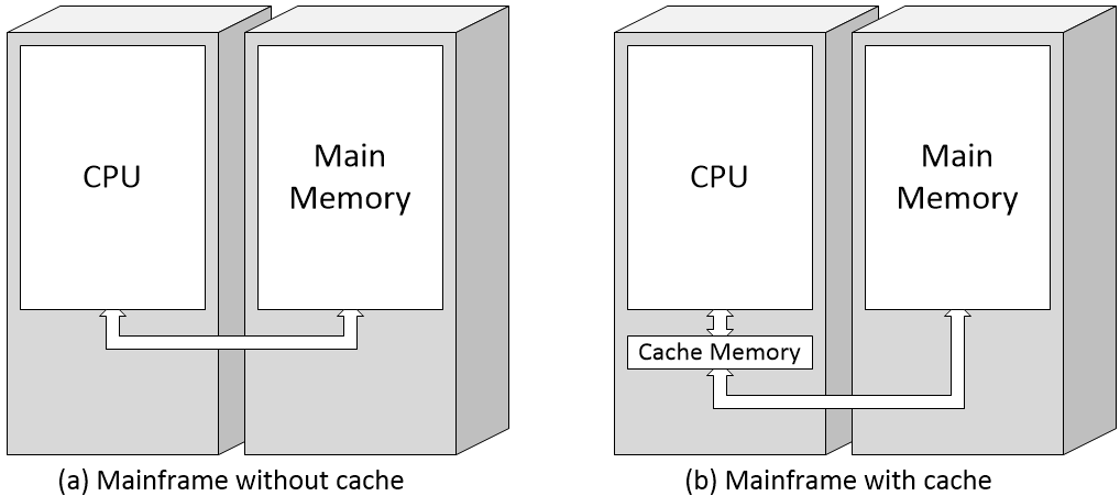
Mainframe without cache memory (left) and with cache memory (right)
(Image source: Max Maxfield)
The cache is a relatively small amount of memory that’s implemented in the fastest technology available (“damn the power consumption”) and that’s located as close to the CPU as possible. In fact, the cache is usually considered to be part of the CPU; the reason I’m showing it as being separate is to simplify the diagrams that are to come.
It should be noted that the above illustration is a gross simplification at best. For example, when the CPU first requests a piece of data from the main memory, that data will be simultaneously loaded into both the CPU and the cache (not “through” the cache as is implied by my illustration). If the CPU requests the same piece of data a second time, it will come from the cache (assuming this entry hasn’t been overwritten by something else in the meantime). If the required data is in the cache, we call this a “cache hit.” If the required data is not in the cache, we call this a “cache miss.” When the CPU wishes to store the result from a computation, that data may be written to both the cache and the main memory at the same time, in which case we use the term “write-through.” Alternatively, the data may be initially written only to the cache, with writing to the main store being postponed until that portion of the cache is about to be overwritten, in which case we use the term “write-back” (or “write-behind”).
There are all sorts of tricks involved here. For example, when a program accesses one piece of data from the main memory, it will oftentimes wish to access other pieces of data located in close proximity (that is, in nearby memory locations). Thus, in addition to copying the requested data into the cache, the system may also “prefetch” other pieces of data that may soon be of interest. Similarly for instructions. In fact, what we’ve shown as a single cache is typically split into two entities: a data cache and an instruction cache.
The first commercially available mainframe computer with a cache memory was the IBM System/360 Model 85, which was announced in January 1968 and first shipped in December 1969. Early microprocessors didn’t have caches. By comparison, to the best of my knowledge, the first microprocessor to boast an on-chip cache was the C100, which was introduced by Fairchild Semiconductor in 1986. The C100 was based on a 32-bit RISC-like instruction set architecture (ISA) called the Clipper architecture.
As an aside, the Intel 386, which was introduced in 1985, could support an external (off-chip) cache of 16 to 64KB (this was sometimes called a Level 2 or L2 cache, even though there was no Level 1 or L1 cache). This was followed in 1989 by the Intel 486, which did support an on-chip L1 cache of 8 to 16 KB.
Unbeknownst to other microprocessor manufacturers, Fairchild Semiconductor patented the concept of microprocessors having on-chip caches. This nugget of knowledge may have slipped through the net when Fairchild sold the Clipper architecture and associated patents to Intergraph Corporation in 1987. You can only imagine the surprise and consternation of the other microprocessor manufacturers — all of whose high-end microprocessors flaunted on-chip caches by this time — when they eventually discovered that Intergraph was sitting in the catbird seat on the cache patent front, as it were, but that’s a story for another day.
As things became more complex over time, designers started to add more levels of cache, which they named L1 (Level 1), L2 (Level 2), L3 (Level3) and so forth. In this case, the L1 cache will be the smallest and fastest and closest to the CPU. The L2 cache will be larger than the L1, but possibly not quite as fast and possibly consuming less power per bit. Similarly, the L3 cache will be larger than the L2, but — once again — possibly not quite as fast and possibly consuming less power per bit. In fact, modern high-end embedded, desktop, and server microprocessors may have as many as six types of cache (the mind boggles).
As another aside, some modern CPUs also often have a teeny-tiny “L0” cache. Typically just a couple of KB in size, this is used for storing micro-operations (micro-ops or µOPs) and is accessed directly by the CPU’s functional units.
For the purposes of these discussions, let’s assume we have only three levels of cache. You may be envisaging this as a simple stack, with the CPU at one end, the L1, L2, and L3 caches in the middle, and the main memory at the other end. If so, I envy you. I remember when I was young and innocent also. The problem is that we are often faced with multi-core processing systems and hierarchical memory subsystems. For example, let’s consider a portion of a System-on-Chip (SoC) featuring two processor clusters, each containing four CPU cores. In this case, we might be looking at a memory hierarchy as illustrated below:
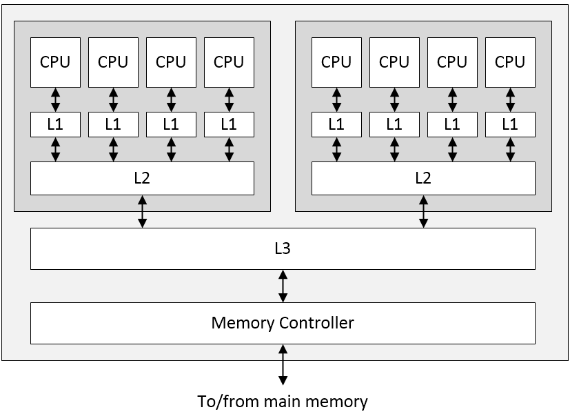
Portion of an SoC showing two processor clusters, each with four processor cores, along with L1, L2, and L3 caches (Image source: Max Maxfield)
Once again, remember that everything we are showing here is simplified to the nth degree (also remember that we can have both instruction and data caches, for example). The next problem we need to worry about is cache coherence (a.k.a. cache coherency). In a multiprocessor system as illustrated above, it’s possible to have many copies of shared data: one copy in the main memory and one in the local cache of each processor that’s requested it. When one of the copies of data is changed, the other copies must be updated to reflect that change. Cache coherence is the discipline that ensures that the changes in the values of shared data are propagated throughout the system in a timely fashion.
Like most things, this sounds simple if you speak loudly and gesticulate wildly, but it’s actually a rather tricky topic to the extent that entire books have been written on this subject. All of which leads us to the question of verification. If you are part of a team designing an SoC of the type illustrated above, how can you verify that your design will maintain cache coherence when it’s being hit hard by real-world workloads?
You might decide to craft a suite of tests by hand, but how do you know if you’ve verified all of the corner cases? One verification approach that has been very successful in general is to use constrained random sequences of stimuli, but this approach doesn’t work well when you have systems as complex as the ones we’re talking about here. The issue in this case is that you start with the stimuli and work your way through all possible combinations and permutations of circuit states until you reach the outputs, but if you are considering every possible thing that might happen, this may result in somewhere in the order of 10^60 test paths, which is a silly number.
Over the lifetime of the project, we might manage 10^4 test cases in simulation, maybe 10^5 in emulation, and possibly 10^6 or 10^7 post-silicon. So, the task of verification engineers attempting to perform system-level verification on the SoC is to run 10^5 experiments out of a space of 10^60 and guarantee there are no bugs. That’s a big ask. They had better pick good samples.
It’s generally accepted that around 70% of an SoC development project will be spent creating verification tests and then running them and debugging the SoC in question. A large portion of this effort is going to be spent verifying cache coherency.
Happily, there is a solution. I was just chatting with David Kelf, who is the CEO, and Adnan Hamid, who is the President and CTO of Breker Verification Systems. We talked about so many things and touched on so many topics that my brain started to leak out of my ears, so it may be best to summarize things as follows. Consider the following illustration.
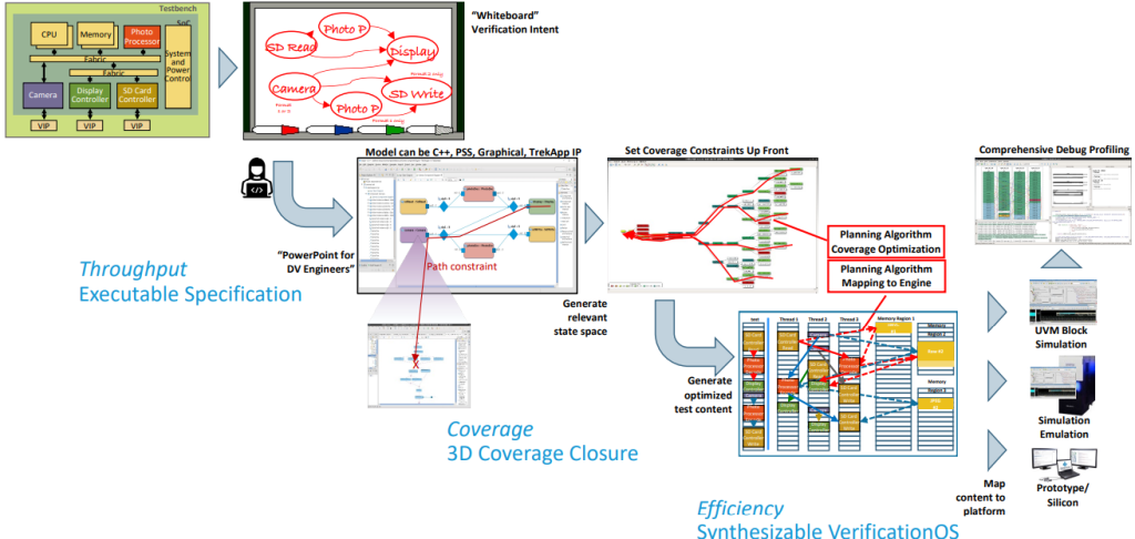
AI-planning-algorithm-driven test suite synthesis (Image source: Breker)
An SoC design is shown in the top left. A typical verification process will involve the verification engineers using a whiteboard to capture a high-level flow diagram of the verification intent. In the past, they would have used this as the starting point for handcrafting their suites of tests. By comparison, in the Breker world, they will capture the same verification intent as an executable specification.
Breker’s tool then uses the executable specification to determine all the paths from the possible input states to the possible output states. Then we come to the clever part: using artificial intelligence (AI) techniques, the system starts at the desired outputs and works out what it will take to achieve them. As part of this, it determines which tests will require shared resources and which can be performed concurrently. There are multiple scenarios, but one of the most interesting to me is that the system can output C code to run on the processor cores coupled with transactions to be applied to the SoC’s inputs/outputs (I/Os). One measure of this approach’s success is to compare the efficacy of handcrafted tests versus those created using Breker’s Cache Coherency TrekApp tool.
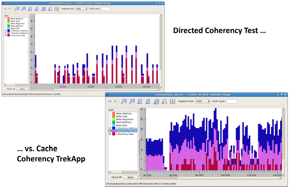
Efficacy of the Cache Coherency TrekApp (Image source: Breker)
I think this is pretty much what you’d expect to see. In the case of the directed coherency tests that were created by hand, there’s only a limited amount of concurrency because that’s all the verification engineers can wrap their brains around. By comparison, the Cache Coherency TrekApp generates a wealth of concurrent tests that really stress the system.
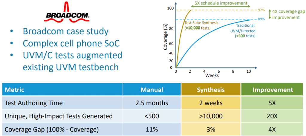
Adnan and David also walked me through a real-world Broadcom case study involving a complex cell phone SoC. It seems that a very competent verification engineer had spent 2.5 months generating ~500 unique, high-impact tests, but that these tests resulted in only 89% coverage. The customer wasn’t satisfied and demanded more, at which point Breker leapt into the picture with a fanfare of sarrusophones (once heard, never forgotten). Using their executable specification technology, in only two weeks, Breker synthesized a suite of more than 10,000 tests that achieved 97% coverage.
Typical user results (Image source: Breker)
Don’t ask me about the amusing reverse-logarithmic-esque scaling on the vertical axis because I don’t have the time or energy (or words) to explain it.
This is probably a good time to mention that the Cache Coherency TrekApp is just one member of a family of TrekApps, each of which targets different aspects of the design. Other members include the ARM TrekApp, RISC-V TrekApp, Power Management TrekApp, Security TrekApp, and Networking TrekApp.
The reason this is such a good time to mention all these TrekApps is that, at the recent Design Automation Conference (DAC), which was held in San Jose, California, in December 2021, Breker unveiled their latest and greatest TrekApp — the System Coherency TrekApp. This basically provides verification engineers with a unified framework that allows them to run the Cache Coherency TrekApp in conjunction with other TrekApps so as to verify the interactions between cache coherency and power and security and interrupts and… I’m exhausted… I can say no more…
…except…
…I’ve recently been doing some work with cloud service providers and hyperscale data centers featuring disaggregated services like racks of processors and other racks of memory, with herds of rampaging virtual machines being migrated from one server to another while running without interruption. If you think maintaining cache coherency is difficult on a single SoC, imagine the problems involved in this sort of cloud center scenario, where you could have virtual machines with multiple caches scattered across multiple processing nodes. Just to increase the fun and frivolity, you can have data in flight between nodes. Obviously, it’s got to be a good idea to verify that everything will work as planned before (a) actually implementing the architecture and (b) having customers and their virtual applications scampering all around.
Then I started to think about Breker, which began life working at the semiconductor level and is now happily bouncing around at the firmware level. It struck me that Breker’s executable specification approach could be extended to these higher-level architectural scenarios.
“Hmmm,” I thought, “This evolution of Breker’s technology could be of interest to a lot of players, including those who create Electronic Design Automation (EDA) tool suites and those who manufacture the processors and other chips that power these hyperscale environments.”
I made so bold as to voice my meandering musings to Adnan and David. This resulted in something of a pregnant pause, after which I was briskly informed that this was possibly “an excellent time to provide a resounding ‘No Comment.’” I wonder if that means they think it’s a silly idea.
I really should point out that I’ve only scratched the surface with respect to describing the capabilities of Breker’s technology. If you are interested in learning more, be assured that the guys and gals at Breker would delight in telling you all about the bits I missed out on. In the meantime, what do you think about what you’ve heard thus far?


