


“A clear conscience is usually the sign of a bad memory.” – Steven Wright
Quick! What is this a picture of?
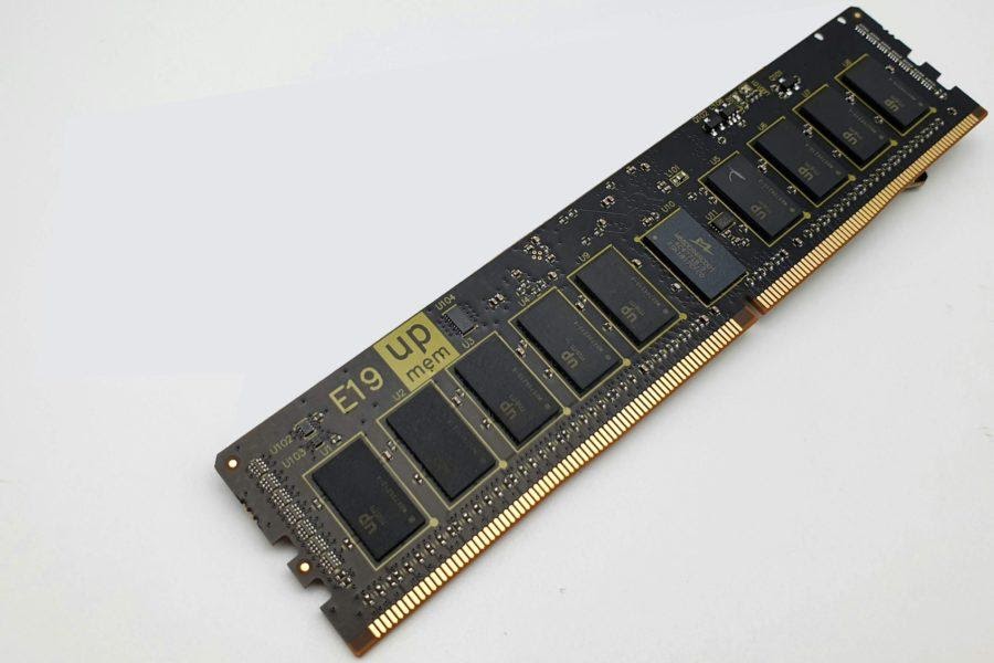
It’s a DRAM module, right? Well, that’s only partially correct. It is a standard DIMM (dual inline memory module), but it’s also 128 microprocessors. Don’t see the sea of CPUs? That’s because they’re coming from… inside the housing!
That’s right: the memory and the processor are one and the same. It’s a smart memory. Or a CPU with a really big local RAM. French startup Upmem calls it a PIM: processor in memory.
The idea is both new and not new. Plenty of computer architects and engineers have lamented the fact that moving data into and out of a CPU consumes a lot of time and a lot of energy. Our hyper-expensive Xeon processors spend a fair amount of their precious time just waiting for the %$@# DRAM to regurgitate data. That’s why we have caches – several levels of caches in the fastest processors.
So, why not move the processor closer to the memory? Or – here’s a crazy idea – put the processor right inside the memory! The bus could be massively wide and infinitesimally short, cutting latency and reducing power consumption! It’ll be great!
Except… Except that anyone who’s ever opened a jar of silicon and sharpened their X-Acto knife knows that you can’t just mix DRAM and logic. They’re incompatible processes. DRAM transistors are designed to be very small (in the horizontal direction) and relatively slow. Logic processes are designed to be fast, especially when making speedy CPUs. Combine the two and you get a lousy CPU surrounded by lousy DRAM. Yuck. Plenty of companies have tried this before (Berkeley’s IRAM is just one example, and we covered others last year), but nobody could ever make it work. Or, more accurately, nobody could ever make it commercially successful. Like an exotic zoo animal, they were fun to look at, but you wouldn’t want to take one home.
Upmem thinks it’s shaken off that curse and come up with an intelligent RAM that’s both workable and sellable. The company says its PIM is good for massively parallel tasks, such as database searching, genome sequencing, pattern matching, and data analytics. It’s not the right CPU for running Linux or for replacing your x86, ARM, or Power processor. Think of it more as an accelerator to complement your main CPU, not to displace it.
On the outside, Upmem’s PIM looks just like a normal DRAM chip, and that’s deliberate. The company sells them as a set of 16 chips on a single module, which you plug into your motherboard like any DIMM. Apart from some BIOS tweaks to awaken its hidden army of processors, no system changes are required. It looks and operates like a DDR4-2400 DIMM, and at first glance you’d never know there was anything special about it.
Inside, however, each of the 16 chips includes 8 processors, for a total of 128 CPUs per DIMM. Most motherboards have multiple DIMM slots, so it’s not hard to imagine a system with a thousand of Upmem’s processors whirring away, cracking those hard AI problems.
The processor itself is nothing you’ve never seen before. It’s a proprietary design created by Upmem specifically for this application. The company briefly courted the idea of embedding ARM or RISC-V processors in DRAM, but quickly decided – as others have – that the compromises would be too great. So, it created a new CPU architecture from scratch with the unique demands of DRAM residency in mind. The result is a nice, tidy 32-bit instruction set that’s programmable in C but binary compatible with nothing. No problem, since it’s intended as an accelerator, not a main processor that needs to run an operating systems or third-party apps.
The processor is fairly basic as such things go, with an emphasis on loop-oriented and data-intensive code. It’s strictly scalar – that is, no parallel or out-of-order execution – but it does support multithreading. It sort of has to, given its usage model. The instruction set is weighted toward shift, rotate, and logic instructions good for transforms. It also supports zero-overhead looping and zero-delay branches with conditional execution. There’s no floating-point support, and the ALU is optimized for single-cycle 8×8 integer multiplies. You get to decide whether it operates in big- or little-endian mode.
At 14 stages, the processor has a remarkably long pipeline for such a slow CPU. Fully three stages are dedicated to instruction fetching, three more are needed to read operands from the register file, and ALU operations take four stages.
Upmem says its PIM runs at about 400–500 MHz, or about one-sixth the frequency of the DRAM on which it sits. For comparison, an ARM Cortex-A8 with a similar number of stages can run at 1 GHz and above. But that’s assuming the ARM is fabricated using an optimized logic process, not a DRAM line that hates logic gates.
Upmem said from the beginning that they wanted to use only standard, unadulterated DRAM processes, not some company-special hybrid that could be fabricated by only one or two licensed foundries. That decision should make PIM easier to build (and sell), but it does force compromises in the design. The long pipeline and unique ISA just highlight those challenges.
Ironically enough for a processor that’s swimming in DRAM, there are two local SRAMs for each processor core. Each core fetches instructions from its own private 24KB of SRAM, and data lives in a 64KB local block. These are equivalent to the local RAM or the “tightly coupled memory” (TCM) found in many MCUs. Upmem decided not to add caches to the PIM because caches require high-speed logic in the critical path for tag lookup. Caches also complicate multithreading, as code gets swapped in and out. Basic SRAMs were simpler and provided much of the same benefit. Plus, they’re deterministic.
An autonomous DMA (direct memory access) engine moves data between the two SRAMs and the big DRAM array via its own 64-bit bus. The DMA is triggered automatically during instruction fetch and decode, so the PIM processor doesn’t have to explicitly tell it to do so.
It’s counterintuitive, but the eight processors in each PIM chip (128 processors per DIMM) don’t communicate in any way. There’s no exotic network or mesh to coordinate their behavior. They don’t share data or instructions. Each one is independent, and you’re welcome to program each one with an utterly unrelated task.
That’s not likely in practice, however. The whole point of having 128 accelerators buried inside your DRAM is to get them cranking on a single big dataset. So, how do you program this thing, anyway?
The processors themselves are hidden from view, accessible only via a handful of memory-mapped registers. You program them by loading code into the DRAM over the normal DDR4 interface. The internal DMA then snags the code and pushes it into each processor’s local SRAM code store. Whatever results they produce are left in the local SRAM data store, which the DMA then moves to the main DRAM array, where it’s visible to your system’s main processor(s).
Because there’s no communication among PIM processors, it’s up to the host CPU to coordinate their actions. Upmem calls this “orchestration,” and it’s a nontrivial task. You’ve got to load the appropriate data where the processors can see it, push the relevant code to each one, and somehow divide up the task in a sensible manner.
Fortunately, Upmem provides a software library to make this as easy and invisible as possible. The SDK (software-development kit) for various Linux derivatives is available on the company’s website. A cloud-based software simulator and an FPGA board with 256 processors are also online.
A weird side effect of dividing processors across DRAM chips is that the data is organized wrong. Normally, each DRAM sits on a single byte of the data bus. When you store a 64-bit word, for example, eight separate DRAMs each get a piece of it. That’s not what you want when you’re asking processors inside those DRAMs to work on a parallel problem. So, one of the built-in functions of the SDK is transposing data from a “horizontal” to a “vertical” orientation so that each PIM processor gets a whole 64-bit word, not just a slice of it.
Upmem is shipping limited quantities of its 4-Gbit PIM chips now, with volume expected later this year. Pricing isn’t public, but the company described it as “almost, but not quite, the cost of a standard DRAM.”
Company CEO Gilles Hamou also said there’s “no emergency” to produce higher-capacity versions that keep up with the DRAM treadmill, nor to advance the current 400-MHz frequency. “Even at 100 MHz, [programmers] would be happy with the acceleration,” he says.
Part of the problem is power. To remain fully compatible with normal DIMMs and standard motherboards, Upmem has to keep its power requirements modest. That’s tough to do when you’re packing in over a hundred processor cores, dozens of SRAMs, and a lot of additional logic. Upmem says that all that content increases die area by about 50% over the DRAM alone. No small task.
PIMs are secret weapons that require no additional real estate, just some BIOS tweaks and a new software library to coordinate their actions. The hardware is a drop-in, but the software isn’t. Still, those 128 accelerators – and that’s per DIMM slot – can provide some impressive speedup for the right set of problems. After all these years and many false starts, Upmem may have finally cracked the processor-in-memory bottleneck.


