

Just to ensure we’re all tapdancing to the same drumbeat before we leap into the fray with gusto and abandon, let’s briefly remind ourselves that in Part 1 of this miniseries we introduced the concept of switch bounce. Later, in Part 2, we took a deeper dive into the bouncing associated with a single pole, single throw (SPST) toggle switch and a single pole, double throw (SPDT) toggle switch.
In Part 3, we started to consider hardware solutions to switch bounce, commencing with the idea of using an RC network followed by a Schmitt trigger to debounce an SPST toggle switch. Most recently, in Part 4, we looked at using a variety of monostable multivibrators to debounce SPST toggle switches, including taking a 555 timer and configuring it to act as a monostable. Sad to relate, we eventually concluded that using monostable multivibrators was not a good way to go.
If any of this stuff is unfamiliar to you, then you might want to take a look at my associated Switch Types and Switch Terminology columns. Also, remember that toggle switches, rocker switches, and pushbutton switches all exhibit switch bounce in pretty much the same way. In fact, the only switches that don’t bounce are the ones most of us rarely, if ever, use, such as mercury tilt switches.
Switch Bounce on an SPDT Toggle Switch
Out of all the hardware solutions we’ve pondered thus far, using an RC network with an SPST switch is my favorite, but this is non-optimal for a variety of reasons, not the least that a full-up solution requires a capacitor, two resistors, a diode, and a Schmitt-triggered inverter (or buffer). There’s also the fact that this adds an element of delay into the proceedings; that is, the time from when the switch is initially activated/deactivated to when the microcontroller (MCU) gets to “see” the transition. (As we discussed in Part 4, whether or not this delay is a problem depends on the application.) Furthermore, the RC values have to be selected to address worst-case bounce times, but these vary from switch to switch. They even vary with the same switch, depending on environmental conditions like temperature and humidity, or just the fact that the switch feels like being #$%^& awkward.
The bottom line is that, although SPST switches are cheap-and-cheerful in the grand scheme of things, they may not be the best option if you wish to debounce your switches using a hardware solution. The next step up the ladder, in terms of switch debounce sophistication, is to use an SPDT component. Let’s briefly remind ourselves as to the bouncing characteristics associated with such a device as illustrated below:
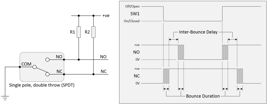
Switch bounce on an SPDT toggle switch (Image source: Max Maxfield)
As per our previous discussions in earlier columns, we are assuming our switch is of the break-before-make (BBM) category, also known as a “non-shorting switch,” which is the most common flavor. As discussed in my Switch Terminology column, this means the moving contact breaks the existing connection with the current throw before making a new connection with the other throw.
What the above illustration is telling us is that we first see bouncing on whichever terminal is breaking (opening), followed by a short “inter-bounce” delay, followed by bouncing on whichever terminal is making (closing).
From Jack Ganssle’s Guide to Debouncing column, we know that — based on the collection of switches he tested — the average and maximum bounce durations were 1.6 ms and 6.2 ms, respectively. How about the inter-bounce delay? Well, the only empirical value I have for this is 2.25 ms, which was measured on the single toggle switch my chum David Ashton used in his column on SPDT Switch Debouncing with an SR Latch.
Debouncing an SPDT Switch with a Dual Inverter Latch
In electronics, a latch is a circuit that has two stable states and can be used to store state information. The circuit can be made to change state by signals applied to one or more control inputs and will have one or two outputs (see also Registers vs. Latches vs. Flip-Flops).
Excluding any control signals, let’s start by considering a latch formed using two inverters as illustrated below. For this sort of thing, Q is regarded as being the “true” or main output, while QB carries the opposing logical value and is referred to as the complementary output.
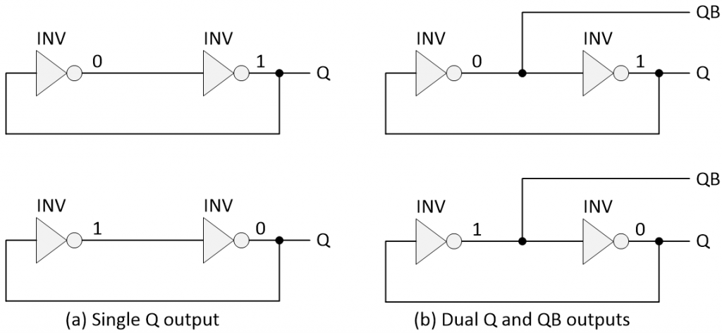
Latch formed using two inverters (Image source: Max Maxfield)
If the output from one of the inverters is a 0, then this will cause the output of the other inverter to be a 1, which — in turn — will cause the output of the first inverter to be a 0. Alternatively, if the output from one of the inverters is a 1, then this will cause the output of the other inverter to be a 0, which — in turn — will cause the output of the first inverter to be a 1.
The main thing to wrap our heads around here is that, whatever values are being outputted by the inverters, the situation will remain this way unless we do something to change it (using our non-existent control signals).
Another way of drawing this circuit would be as illustrated below. Observe that these new illustrations are functionally identical to our earlier version. All we’ve done is to move things around a bit, but this new version may make it a bit easier to understand what’s going on. Whatever logic value is coming out of one of the inverters will cause the other inverter to generate the opposing value.
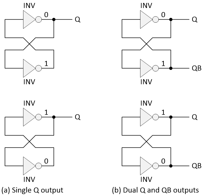
Another view of a latch formed using two inverters (Image source: Max Maxfield)
So, how do we persuade our latch to change its state? We need to add some control signals, and one way to do this would be to use an SPDT switch as illustrated below (observe that we’ve also added current-limiting resistors to prevent the inverters’ outputs from trying to source too much current).
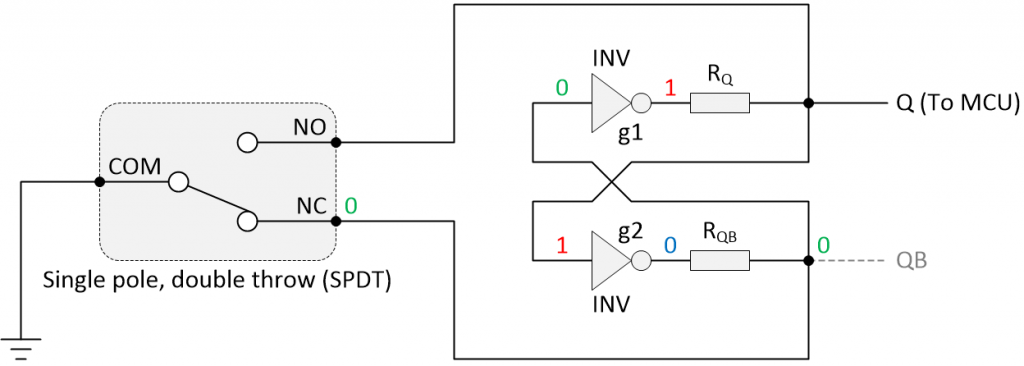
Debouncing an SPDT Switch with a Dual Inverter Latch (Image source: Max Maxfield)
The reason I’ve shown the QB output as being grayed out is that it’s available if we ever want to use it, but we don’t actually need it in this case because the Q output is a debounced signal that can be passed to the MCU
How does this work? Well, let’s assume that we start with the switch as shown in the above illustration; that is, with the NC (“normally closed”) terminal connected to ground, or logic 0 (shown in green). This means the QB output is being pulled down to a logic 0 (shown in green), which causes inverter g1 driving the Q output to generate a logic 1 (shown in red). In turn, this causes inverter g2 driving the QB output to generate its own logic 0 (shown in blue).
When we toggle the switch, the first thing that will happen is that the NC contact will bounce, but all it’s really doing is bouncing between logic 0 and a tristate condition (we don’t have, or need, any pull-up resistors in this circuit). This means the bouncing on the NC contact doesn’t have any effect on the existing value stored in the latch.
After the inter-bounce delay, the NO (“normally open”) contact will start to close (and bounce, of course). When it does close, it will pull the Q output down to a logic 0, which will cause inverter g2 driving the QB output to generate a logic 1. In turn, this will cause inverter g1 driving the Q output to generate a logic 0. Now, when the NO contact bounces, all it’s really doing is bouncing between logic 0 and a tristate condition, which doesn’t affect the new value that’s just been stored in the latch.
Debouncing an SPDT Switch with an SR Latch
One reason the latch formed using two inverters discussed above was of interest as a hardware switch debounce solution in the “early days” (circa the early 1960s) is that each inverter could be implemented using a single bipolar junction transistor (BJT) and a resistor, or using the combination of two field-effect transistors (FETs) in the case of CMOS. This was something to think about in the days when the cost of individual transistors was a significant consideration.
On the downside, forcibly pulling the output of a logic gate to ground lacks a certain “finesse,” shall we say. As an alternative, many people regard the combination of an SPDT switch with an SR latch to offer the crème de la crème of hardware debouncing solutions. For example, consider a NAND gate implementation as illustrated below:
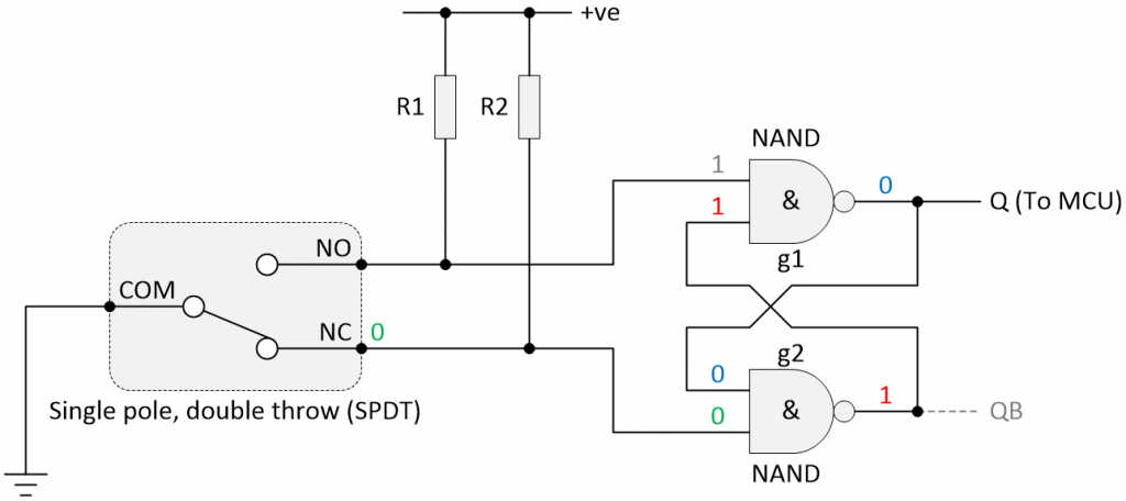
Debouncing an SPDT Switch with a NAND-based SR latch starting with the switch’s NC contact connected to ground (Image source: Max Maxfield)
Once again, let’s take this step-by-step. Let’s assume that we start with the switch as shown in the above illustration; that is, with the NC terminal connected to ground, or logic 0 (shown in green). If any of a NAND gate’s inputs are logic 0, its output will be logic 1. Thus, the logic 0 (green) on NAND gate g2’s input drives its output to logic 1 (shown in red).
In turn, this means that both of the inputs to NAND gate g1 are logic 1 — one from pull-up resistor R1 that’s connected to the switch’s NO terminal (this 1 is shown in gray) and one from NAND gate g2 (this 1 is shown in red). If both of a NAND gate’s inputs are logic 1, its output will be logic 0. Thus, the two logic 1s on NAND gate g1’s inputs drive its output to logic 0 (shown in blue).
Observe that the logic 0 coming out of gate g1 is fed back to the input of gate g2 (also shown in blue). This is important, because when we toggle the switch, the first thing that will happen is that the NC contact will bounce. In this case, it’s potentially bouncing between a logic 0 (from its COM terminal) and a logic 1 from pull-up resistor R2 that’s connected to the switch’s NC terminal. The point is that the blue logic 0 from gate g1 will continue to force gate g2 to generate a 1 on its output.
Now consider the illustration below. Following the inter-bounce delay, the NO contact will start to close (and bounce, of course). Once again, if any of a NAND gate’s inputs are logic 0, its output will be logic 1. Thus, the logic 0 (green) on NAND gate g1’s input drives its output to logic 1 (shown in red).
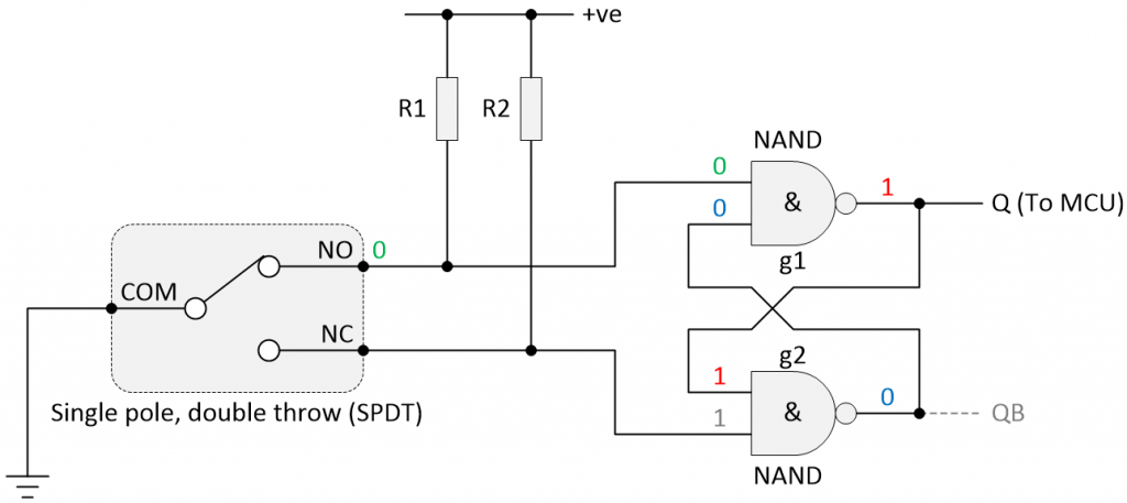
Debouncing an SPDT Switch with a NAND-based SR latch (Image source: Max Maxfield)
In turn, this means that both inputs to NAND gate g2 are now logic 1 — one from pull-up resistor R2 that’s connected to the switch’s NC terminal (this 1 is shown in gray) and one from NAND gate g1 (this 1 is shown in red). And, once again, if both of a NAND gate’s inputs are logic 1, its output will be logic 0. Thus, the two logic 1s on NAND gate g2’s inputs drive its output to logic 0 (shown in blue).
And, of course, the logic 0 coming out of gate g2 is fed back to the input of gate g1 (also shown in blue). This is important, because even though the NO terminal is currently bouncing, this logic 0 will continue to hold gate g1’s output at a logic 1.
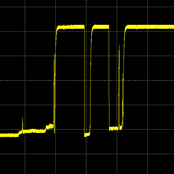
What does this look like in the real world? Well, take a look at the oscilloscope screenshot from David Ashton’s SPDT Switch Debouncing with an SR Latch column as illustrated below.
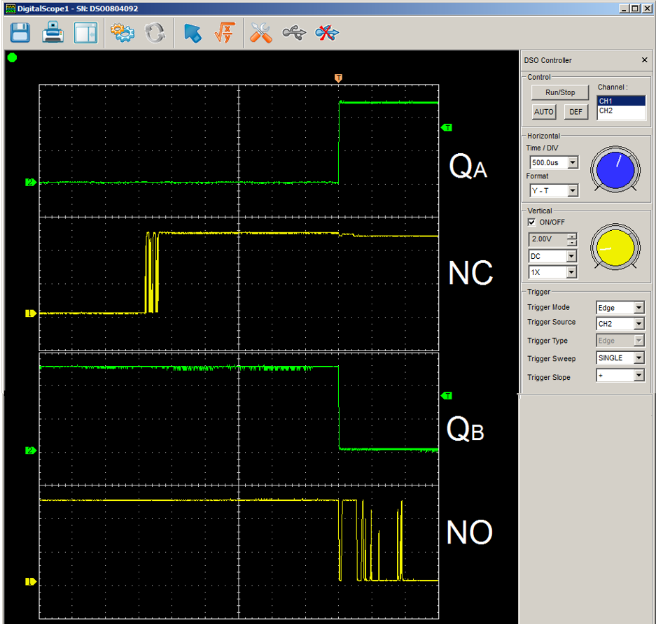
Relative timings of debounce circuit. The first NO make toggles the bistable. (Source: David Ashton)
In this case, David called our Q and QB outputs QA and QB, respectively, but “A rose by any other name would smell as sweet,” as the Bard would have it.
We commence with the switch’s NC terminal connected to ground. The first thing that happens when we start to toggle the switch is that the NC terminal bounces while breaking contact, but this has no effect on the QA and QB outputs. This is followed by the inter-bounce delay, during which nothing happens, in order to build the excitement. It’s only when the switch’s NO contact makes its first transition to ground that the QA output transitions, quickly followed by the QB output. As we see, this all happens almost instantaneously (the delays associated with these gates are only a few nanoseconds). As we discussed above, any subsequent bounces on the switch’s NO terminal have no effect on the state of the latch (and thus on the QA and QB outputs).
This SPDT switch and RS latch combo provides such a good hardware switch debounce solution that it was favored by the designers of IBM’s mainframe computers circa the 1960s. Purely for the sake of completeness, we should note that it’s also possible to use a NOR gate SR latch implementation as illustrated below:
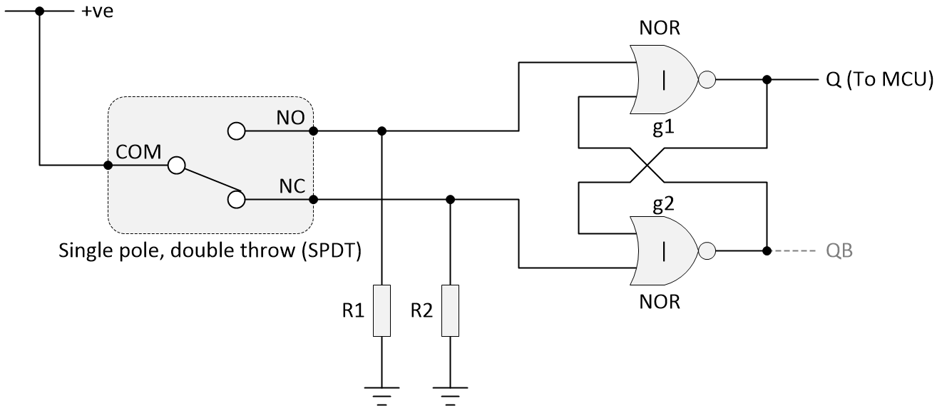
Debouncing an SPDT Switch with a NOR-based SR latch (Image source: Max Maxfield)
Debouncing SPDT Switches with D-type Latches and Flip-Flops
A lot of people are confused as to the difference between latches and flip-flips. If you find yourself a tad “fluffy” in this area, may I make so bold as to recommend my Registers vs. Latches vs. Flip-Flops column.
As we discussed in Part 3, there are historical reasons why the early solutions to switch debouncing were hardware-based. One of the points we considered was that printed circuit boards (PCBs) circa the 1970s could contain hundreds of 74xx chips, where each of these devices typically contained a handful of jellybean logic gates or functions.
Almost invariably, there were functions left unused — a NAND gate here, an SR latch there, perhaps even a D-type latch or flip-flop that was unaccounted for. Hardware design engineers saw these uncommitted logic functions as being “fair game” for use in debouncing their switches.
As one example, consider a positive-edge-triggered D-type flip-flop with active-low asynchronous Preset (a.k.a. Set) and Clear inputs as illustrated below:
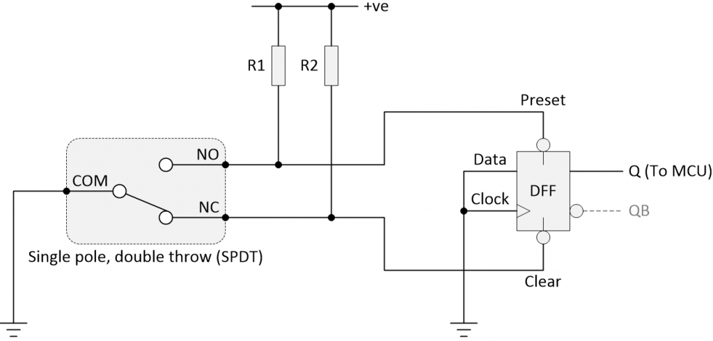
Debouncing an SPDT Switch with a D-type flip-flop (Image source: Max Maxfield)
Observe that the flip-flop’s data and clock inputs would be “tied off” to ground to prevent any noise from spuriously triggering the device.
The thing to remember here is that the output stage of a D-type latch or flip-flop is basically an SR latch, and that the Preset and Clear signals feed directly into this latch. I don’t know about you, but I’m constantly amazed by the ingenuity of the designers of yesteryear.
Next Time…
I tell you, when I started out on my quest to waffle* about switch debounce, I had no idea how much work it was going to be. (*It’s widely acknowledged that, if you end up embarking on a quest, then a “waffling quest” is the best of all options.)
Happily, the end is in sight. In my next (hopefully, final) column on this topic, we will consider special switch debouncing chips, debouncing solutions for FPGAs, and software solutions for microcontrollers. Until then, as always, I welcome your comments, questions, and suggestions.


Max
I thought I could point out to your readers who intend to use cross coupled NOR or NAND gates, that there are old CMOS parts, the CD4043 and CD4044, that include 4 such configurations allowing for 4 denounced switches per 16 pin IC. As I recall, they also have 3-state outputs allowing them to be bussed, possibly saving on micro input pins- something to really consider in ye goode olde days
Hi Aubrey — thanks for the reminder. The funny thing about all of this is that — looking back –I’ve never learned anything that didn’t eventually come in handy one day or another (the real trick is to use it before I forget it LOL). As we’ll see in my next column, debouncing in software can be tricky for beginners and hobbyists (so many things to think about), so a cheap-and-cheerful SR Latch may make sense, especially if you can get a lead through-hole (LTH) component that will plug into a breadboard.
In case you missed it I left this comment at the first installment of the series.
I have designed a SPST SR Latch debouncer. It tells you – like the SPDT SR Latch circuit – as soon as the switch starts changing state (plus deglitch time). Either opening or closing.
https://spacetimepro.blogspot.com/2023/09/switch-debouncer.html