


We’ve blissfully led separate, siloed lives for years. IC designer? Someone’s having trouble routing from your pads? “Not my problem.” Package designer? Electricals on a particular signal are sketchy? “Not my problem.” PCB designer? Someone doesn’t like that the drive on an output isn’t high enough to drive your signal? “Not my problem.” It’s so much easier when you have a restricted scope, and anything outside that scope is someone else’s problem.
But that’s not gonna work so well going forward if you really want to optimize the interactions between your chip, the chip package, and the PCB (or module board) to which the package will be mounted. And, as we continue to drive up integration and drive down dimensions, the lines between chip, package, and board or substrate are starting to blur.
A signal may start at the output of a transistor, but thence it goes up through a series of contacts, vias, and metal traces to a pad, where it jumps onto an aluminum wire (perhaps) and loops up over to a wireframe or other redistribution layer, where it moves through a ball or bump and onto a PCB trace for some distance until it reaches its destination. Despite all the domain crossings, it’s still all one signal.
Which, of course, means that any problems anywhere now become everyone’s problems. Which could be made easier if design tools also lost their hard boundaries at the chip, package, and board edges.
The focus here is on advanced packaging and modules, a category that Mentor refers to as High-Density Advanced Packaging (HDAP). There are lots of variants out there on such packaging; Mentor includes FOWLP (more in a minute), 2.5-D interposer-based solutions, CoWoS (more in a minute), high-pin-count flip-chip, and system-in-package (SiP).
The motivations consist of both integration and cost. Integration is pretty obvious, but cost? Well, one of the benefits is that you can put together a heterogeneous set of dice – analog, III/V materials, digital CMOS, memory – without the high cost of trying to do a single-chip solution that would use all that technology. Done properly, you end up with a single package with everything in there, just as if it were monolithic, but it houses multiple dice – and even “dielets/chiplets” and passives.
Yeah, that dielet or chiplet notion is new to me. It’s a term I heard from Cadence referring to chips that use only a portion of what might go into a full chip – like a single IP block. It’s almost as if “chip” has now been promoted to mean “SoC-level,” and if you have less than that – like all chips did a decade ago (imagine an entire chip that’s just a mux!) – then it’s one of these special cases. Of course, unlike in the past, here we’re not packaging the chiplet by itself.
Cadence described one surprising new aspect. I’m used to chipmakers creating a die, packaging it up, and then selling it more or less generically to anyone who wants to use it for whichever boards or modules they want. Well, now, apparently, chips and chiplets are being designed specifically for integration together in a module. Those dice would not be purchased by anyone else; only the completed module would be sold.
Are You a Fan?
Before we go further, I’ve honestly been confused about exactly what a couple of newer packaging terms – fan-in and fan-out – mean, and conversations with both Cadence (before DAC) and Mentor (at DAC) helped.
It’s somewhat intuitive – after an explanation (which, of course, means not intuitive at all – especially if you’re used to the meaning of those terms in digital logic). Fan-in wafer-level packaging (FIWLP or FI-WLP) is more commonly known as chip-scale wafer-level packaging (CSWLP). It refers to a situation where a redistribution layer (RDL) routes die signals towards the center of the die into a smallish number of balls for mounting on a board or other substrate. It’s called “fan-in” because peripheral signals get routed inwards.
Fan-out wafer level packaging (FOWLP or FO-WLP) means that the substrate, which was restricted to the chip dimensions in FIWLP, is larger than the chip and may have other chips or passives attached. You can accommodate many more signals, and they’re routed away from the chip – more or less like how PCB layout has always been. Hence “fan-out.”
There’s another FLA (five-letter acronym) that gets tossed about in here as well: CoWoS. This is specifically a TSMC technology that lets you put a chip on another die (which is part of a wafer that hasn’t been diced up yet) and then mount that combination onto substrates. By contrast, FIWLP (or CSWLP) and FOWLP are generic industry terms. (I can’t help wanting to pronounce FOWLP as “foul-up”… or perhaps “fowl-up,” which is what a duck hunter hollers when he sees a duck fly up, right?)
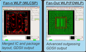 (Image courtesy Cadence; I added red rectangles to highlight die boundaries)
Packaging Analog Modules
So with that simplistic lead-up, we come to our specific announcements. First up, a focus on analog. The need for this is pretty much a no-brainer, really. Pretending that a wire that will exit a die, go through a package, and emerge onto a PC board for further routing – and will have a nice clean break at any of those boundaries is fantasy. Perhaps it used to work, but, as we saw above, we need to look at that not as three wires – on die, in package, and on board – but one single connection. Parasitics anywhere will affect it everywhere.
When you think analog, many designers think Cadence’s Virtuoso. For this topic, they’ve announced Virtuoso System Design Platform. It breaks the barrier between chip and board design so that they can be done holistically.
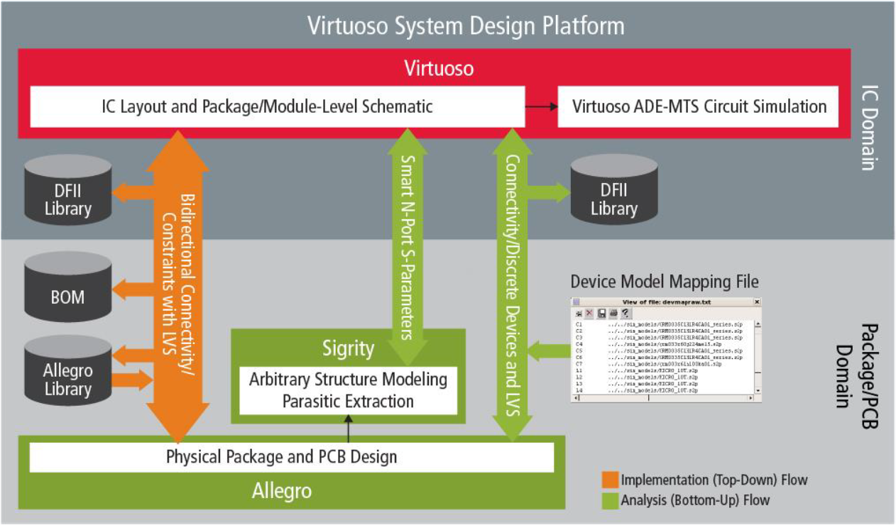 (Click to enlarge; image courtesy Cadence)
All of the connectivity, models, and libraries are managed automatically. They have a top-down approach for implementation, where you’re pulling all of the various pieces together, and a bottom-up approach that focuses on analysis. Digital chips can also be added via Open Access or by importing any other complete die that you might have acquired through some third party. Even discretes can be included, since many vendors will provide a device model mapping file. You then get a physical footprint and a schematic model for the module.
Once done, you’ll run a layout-vs-schematic check. Much of the basic layout that is automatically generated will be correct by construction, but Cadence says that there are still other aspects that need to be checked.
FR-4 and Silicon Compete
In a separate announcement, Mentor introduced a couple of variations on their Xpedition tool for managing HDAP implementations.
As the need grows for tighter routing, you start to exceed what’s possible on a traditional FR-4 (or other organic) board. Silicon, meanwhile, is managing 10s of nanometers – on chips. That level of dimension requires lots of expensive fab equipment, but it’s possible to do better than organics – on the order of 2 or 3 mm instead of 8 or 10 mm – on silicon by printing the lines.
Unlike a die, where you deposit aluminum (or copper) and then etch away the extra, this is an additive process where you “place” the metal exactly where you want it. You can’t get the aggressive pitches that you can do on a wafer, but it’s far less expensive to build.
Mentor lists several differences between the characteristics of organic boards and silicon. This means either that expectations have to change or that tools need to bridge the gap in expectations.
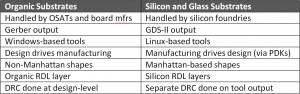
(Source: Mentor)
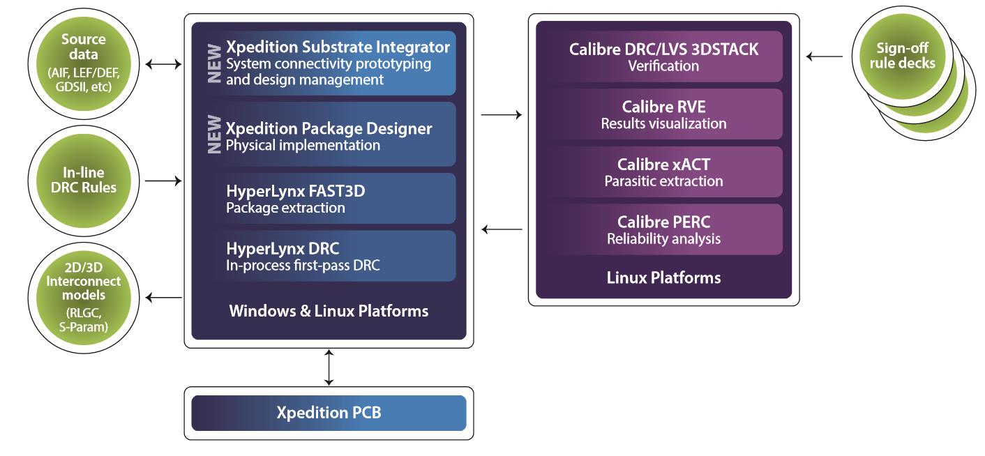
The first Xpedition variant is called Xpedition Substrate Integrator; it’s intended for use by architects and chip designers trying to prototype and figure out the best holistic layout. The second tool is called Xpedition Package Designer, and it’s intended for use by – surprise! – someone designing packages.
 (Click to enlarge; image courtesy Mentor)
PCBs are, of course, part of this whole deal, but there’s already an Xpedition PCB that ties in with this. The three domains interact as illustrated in the following image.
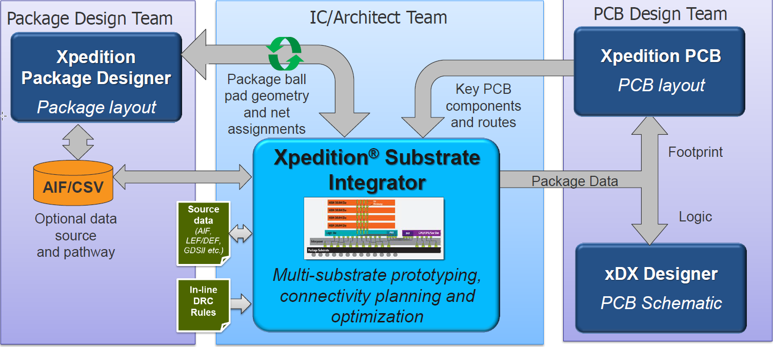 (Click to enlarge; image courtesy Mentor)
Design-rule checks (DRC) are implemented a couple of different ways. There’s a HyperLynx DRC that’s quick and catches around 85% of the issues, according to Mentor. For sign-off, this gets handed off to Calibre. At this low level, everything is in a format that Calibre needs, so no new version of Calibre is needed.
The one catch between Xpedition and Calibre is that Xpedition can run on Windows or Linux; Calibre runs only on Linux. Mentor has resolved this on Windows systems by instantiating a Linux VM for hosting Calibre. This all happens opaquely; you really don’t need to worry about that detail.
Verification also involves more than just the opens and shorts tests that used to suffice. These days, there are other things to check, like ensuring balance of metal density to keep wafers from warping. Yeah, who knew.
These two tools from Cadence and Mentor seem to have different focuses. If I were to zero in on the fundamental verification aspects that each focus embodies, Cadence is about analog electrical verification in the context of an overall integrated module; Mentor is about the layout and DRCs, particularly with respect to silicon substrates. That said, they both appear capable of handling the full flow in conjunction with accompanying tools.
In either case, the walls of the silos are crumbling. Distinct skills are still needed in each area, but now they need to collaborate to get the results they’re looking for in a reasonable amount of time.
More info:
Cadence Virtuoso System Design Platform


What do you think of Cadence’s and Mentor’s tools for integrating dice into advanced packages?