


Most people are familiar with the TNG concept, which sprang from the original Star Trek TV series being rebranded as “Star Trek: The Original Series” when its shiny successor “Star Trek: The Next Generation (TNG)” appeared on the scene (no pun intended). Well, I’ve just been introduced to the next generation (TNG) of design for test (DFT).
In my previous column, Distributed On-Chip Temperature Sensors Improve Performance and Reliability, I blathered, blabbered, and babbled about the functional and timing verification technologies (or lack thereof) associated with my initial ASIC design in 1980. This was my first position after graduating from university. I was a member of a team designing CPUs for mainframe computers at International Computers Limited (ICL) in West Gorton, Manchester, England.
In 1981, two of the managers from ICL left to form their own company called Cirrus Design, and they subsequently invited me to join them. The way we made money in the early days was to write test programs for printed circuit boards (PCBs) using 2225 testers from GenRad.
Most of the boards for which we were creating tests consisted of large numbers of “jellybean” logic integrated circuits (ICs) like the SN54/74-series from Texas Instruments (TI). All we were provided was a PCB that was supposed to be “known good” (but often wasn’t) and a schematic diagram whose revision was supposed to match that of the board (but often didn’t).
So, the first step was to take a WAG (wild-ass guess) as to the intended function of the board, and to then write a test program that would ensure the board was working as desired. One of the things I quickly discovered was that few of the board’s originators had any concept of design for test (DFT). As a result, we often had to be creative regarding bringing internal logic states to the outside world.
The 2225 was classed as a functional tester (as opposed to a bed-of-nails tester). The board to be tested was plugged into the 2225 via its edge connector, which meant the tester had access only to the board’s primary inputs and outputs.
We created our test programs as a series of input test vectors, each defined as a collection of logic 0s and 1s, which were clocked into the board. We also defined a series of expected output vectors, each specified as a collection of 0s and 1s.
These test programs could easily contain thousands, sometimes tens of thousands, of test vectors. Since the boards contained convoluted combinations of combinatorial and sequential logic functions, the expected outputs were delayed by varying numbers of clock cycles on a path-by-path basis.
The next step was to apply a fault to a node of the circuit board, say shorting the output of a logic gate to ground. You’d then run the test program — which compared the expected outputs you’d defined to the actual outputs coming out of the board — to see if it detected the fault. If not, you had to revisit your test program to determine why it failed to detect this fault, and then modify the program accordingly.
You repeated this process for every possible fault you could apply to the board. Oh, the fun we had. But wait, there’s more, because once you were happy with your test program, you had to learn the “signatures” for every node on the board. The idea here is that you provided the 2225 with a text-based netlist of the design. The tester had a “flying probe” on the end of a wire. The tester instructed you to place the probe on the first pin of the first chip, then it ran the entire test program and captured the 0s and 1s on that node. Once again, you repeated this process over and over again for each node on the board.
So, here’s the problem. A board could contain thousands of nodes, and a test program could contain tens of thousands of vectors, so there could be a humongous number of bits of information associated with each node, but memory was very expensive and very limited in those days. The solution was for the tester to use a 16-bit linear feedback shift register (LFSR) to generate a cyclic redundancy check (CRC) for each node, thereby shrinking all of the test data associated with that node into a 16-bit CRC value (called a “signature”) that was assigned to the node.
Now, this is where things got really clever. When a board failed in the field, it was taken to a test center and connected into a 2225 running your test program. The operator ran the program, which determined which output or outputs were providing incorrect signatures. The tester then instructed the operator to place the guided probe on the output of the chip that was driving one of the failing outputs and re-ran the program to ensure that the bad output signature from the chip matched the bad output signature from the board.
The tester then instructed the operator to place the probe on one of the inputs to the chip that could affect the failing output and re-ran the test. If this input signature was ”good,” the tester would move on to the next input. If the input signature was “bad,” the tester would guide the operator to place the probe on the output of whichever chip was driving this input.
Eventually, the tester would either find a chip with bad outputs and good inputs (i.e., the chip had failed) or a track with a good signature on the driving chip and a bad signature on the receiving chip (i.e., the track had failed).
I fear I’m simplifying things a tad, but I hope I’ve managed to convey the gist of the process. I have to say that this was one of the most amazing learning experiences of my life. In addition to honing my logic skills, I was introduced to LFSRs, CRCs, and even a character-encoding technique called Radix 50 that allowed you to store three uppercase alpha-numeric characters in a 16-bit field (see also Tips and Tricks: Compressing Text Characters).
Cirrus Designs had a sister company called Cirrus Computers, which commercialized the HiLo logic simulator that was created by students at Brunel University in 1981. Although the term register transfer level (RTL) wasn’t around at that time, HiLo is now recognized as being the first true RTL simulator.
The next generation of the simulator had three flavors: a logic simulator, a min-max dynamic timing simulator, and an incredibly sophisticated fault simulator. The reason I mention this here is that I started developing simulation models, transferred to Cirrus Computers, and ended up traveling the world giving training courses in logic simulation. It’s also where I first ran into Brian Bailey, who is currently the technology editor for electronic design automation (EDA) at Semiconductor Engineering. It’s amazing to think that Brian taught me all about DFT and SCAN testing and automatic test program generation (ATPG) when much of this was in its infancy more than 35 years ago as I pen these words.
But none of this is what I wanted to talk to you about.
The reason for my waffling in this column is that I was just chatting with the guys and gals at Real Intent. Recently, these little scamps announced their latest and greatest offering, Verix DFT, which is a multimode, full-chip capacity, DFT static sign-off tool.
Test is a huge industry. Tester socket time is very expensive, so anything that can be done to execute a “shift left” and resolve problems as early as possible in the development cycle is considered to be a very good thing indeed. This explains why Verix DFT is best deployed throughout the design process:
- During RTL design as part of fixing asynchronous set/reset, clock, and connectivity issues as early as possible.
- Following scan synthesis to check for scan chain rule compliance.
- Following place-and-route (P&R) to assess and correct issues with scan-chain reordering or netlist modification.
![]()
Verix DFT is deployed throughout the design process (Image source: Real Intent)
In addition to the fact that Verix DFT has full-chip capacity, there are three key aspects to its multimode capabilities that reduce setup times and speed runtimes and decrease the amount of time spent debugging and fixing violations. In a single multimode run, the tool can support:
- Multiple ATPG Partitions: Verix DFT saves substantial time by verifying multiple ATPG partitions in each run, eliminating the time-consuming process of running DFT static sign-off for each partition with each partition requiring its own test mode.
- Multiple Constraint-Sets: Verix DFT uses design constraints to verify DFT sign-off rules for multiple sets of constraints in one run. Each constraint-set corresponds to the types of ATPG patterns, such as uncompressed, compressed, diagnostic, and connectivity.
- Multiple Constraint-Sets Across Multiple Test Modes: The combination of the first two capabilities gives designers the flexibility to verify multiple constraint-sets across multiple test modes.
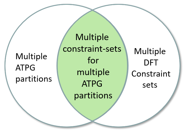
In a single run Verix DFT can handle multiple ATPG partitions and multiple DFT constraint sets (Image source: Real Intent)
Not surprisingly, the folks at Real Intent are rather enthused at the moment. To be honest, it’s difficult to get them to stop talking about all of Verix DFT’s features, functions, and capabilities. So, just to put them out of their misery, I will summarize the key points they really want everyone to know as follows:
- Capacity/Performance: Verix DFT can handle multimillion-gate designs in minutes with full chip capacity and a low peak memory footprint.
- High Coverage Rule Sets: Real Intent uses a comprehensive array of rules to help ensure high coverage at all design stages, including asynchronous set/reset, clock, scan-chain, flip-flop, port & connectivity signoff rules, and a variety of basic setup checks.
- Fine-Grained Rules: The fine-grained rules enable faster identification of specific design fixes.
- Rule Selection & Configurability by Test Mode: Verix DFT’s rules can be selectively enabled in each test mode, such that the different test modes can each have different rules enabled. The severity level (error, warning, or information) is also configurable by test mode.
- Fast Setup: Verix DFT is easy to set up and use, requiring only a few hours, rather than the days or weeks that may be required with other static DFT tools.
- Smart, Tiered Violation Reports: The tool’s accurate, detailed design analysis delivers more precise reporting without duplication. Verix DFT’s violation reporting lets you hierarchically categorize the violations and then toggle to expand or collapse the violation groups. The violations are organized in a tiered priority order, providing guidance to help designers more quickly pinpoint the root cause problems.
- Integrated iDebug: As with all Real Intent static sign-off tools, the folks at Real Intent have integrated their iDebug debugging platform to provide schematics to facilitate DFT check debugging, cross-probing, and easy waivers that can be ported between runs.
- Root-Cause Analysis & Recommended Fixes: The tool labels schematics with rule-specific debug information, such as the glitch sources and the convergence instances for reset glitch rules. The complete debug path is shown for path-based rule violations. Additionally, Verix DFT provides precise user instructions on the setup changes required to fix specific violations.
- Fault coverage estimation: Verix DFT has an additional tool option for fault coverage estimation. When this option is enabled, it will provide fault coverage for each test mode, along with a rollup of overall scan test fault coverage estimation. By automatically estimating the fault coverage for each test mode, the user can better prioritize violation debug order and assess readiness for sign-off.
Phew! I don’t actually do design for test myself anymore, but even I want to play with Verix DFT. For those who are in the test industry, I think the announcement of Verix DFT is going to be interesting news indeed. How about you? Do you get to dip your toes in the DFT waters? If so, it would be great if you’d care to share your thoughts and experiences in the comments below.


Hi Max,
Back in the dark ages (1990/91 timeframe) I had the opportunity to design an ASIC. At that time the existing FPGAs were not big enough or fast enough to handle what I needed to do so I got to dip my toe into ASICs. This was before HDLs were trusted so it was a full-up schematic design. As part of the process I had to develop test vectors that could be used for both software simulations of the design and, later, used to inject live signals into packaged die. The test vectors were specially formatted text files so I got to work with a text editor. By the time I was done I had generated over 1 million vectors (cut and paste got a real workout!). The chips worked properly and the fab facility ultimately adopted the design as their test vehicle. Whenever they changed their process or geometry, they’d do a run of my chip to verify that the new process was OK — all because of those test vectors. They did this for several years until the facility was closed. This was back in the day when geometries were measured in ghastly huge microns. I was working at 1.2, 1.0 and 0.9 microns, or 1200, 1000 and 900 nm for today’s crowd. Creating the vectors was a royal pain back then. Anything that can automate that process and still give good coverage is a total win. I solo designed two ASICs, and co-designed a 3rd before switching completely to FPGAs in the early 90’s. Never looked back.