

I’m starting to fear the world is passing me by. When I designed my first ASIC in 1980, it was a Toshiba gate array device implemented at the 5 µm technology node, which was pretty much state-of-the-art for general-purpose digital ASIC designs at the time.
As I recall, this device contained around 2,000 equivalent gates (2-input NAND gates). My design was captured at the gate and register level using pencil and paper (many, many sheets thereof). Once the design had passed functional verification and timing verification, it was sent to the drawing office to be redrawn by people with sharper pencils and posher stencils.
Logic simulators? Timing analyzers? Don’t make me laugh! Functional verification was performed by gathering other members of the team, laying your schematics on the table, and having them dissect your design with you defending your decisions. Only after everyone was convinced you had a clue did the design progress to logic optimization, which was performed by a quiet guy who had a black belt in optimization techniques and whom we didn’t let out very often.
Following optimization and another round of functional verification, timing analysis was performed by my identifying all of the critical paths and then adding the gate, track, and load delays together by hand on a path-by-path basis. I didn’t even have a calculator.
Eventually, the schematics for the design were handed over to another group that was in charge of performing the layout. After some period of time (I think it was several weeks), I was informed that the layout had been completed. My version was presented as a monstrous text file stored on a magnetic tape. Not that I ever saw the tape itself, you understand; that was kept behind locked doors with its compatriots in the main computer room. But I could access it by issuing a command on my terminal, which caused some minion to scamper through the bowels of the building to retrieve my tape from wherever it was stored and load it onto a reel-to-reel machine, at which time I was informed that the file was ready for my attention.
The next step was to perform a layout versus schematic (LVS) process, which is used to determine whether the integrated circuit layout corresponds to the original schematic or circuit diagram of the design. These days we have computer-aided electronic design automation (EDA) tools for this task. In those days of yore, we could only dream of such technologies.
As I say, my version of the layout was presented as a humongous text file, with different characters indicating things like the areas of P-type and N-type silicon, the various layers of metal, and the vias between layers. The next step was to print this out as multiple strips of fan-fold paper (a.k.a. continuous stationary (UK) or continuous form paper (US)).
As I recall, the layout for this chip required about 20 strips of paper, each about 25 feet long and 15 inches wide. Using a lot of sticky tape and a large room with no furniture and a solid floor, these strips were joined to form a large square 25 feet on each side.
I performed the LVS on my design by walking around the layout in my socks (I didn’t want to tear the paper) carrying my book of schematics and using different colored pencils to mark off each feature in the schematic versus the corresponding feature in the layout. The goal, of course, was to end up with one-for-one matches and everything colored in. The last thing you wanted was to think you’d finished and to then spot an unmarked gate or wire in the schematic or on the layout. Actually, that was the second-to-last thing you wanted — the very last thing you wanted was to have to re-print the layout and start the whole process all over again.
Over the years, technology nodes shrank smaller and smaller. I remember when semiconductor foundries started to approach the 1 µm technology node. Those were exciting times. Of course, the naysayers were out in force trumpeting their belief that 1 µm was the absolute limit beyond which we could not tread (“Boldly going behind the beyond, behind which no man has boldly gone behind, beyond, before,” as Captain James T. Kirk might have said after a few too many glasses of Klingon prune juice). And, of course, the physicists and scientists and engineers paid the naysayers no heed, continuing on their merry way through the 0.8, 0.35, 0.18, and 0.13 µm technology nodes.
Eventually, we all got tired of saying things like “How exciting Cuthbert, we’re at the ought point one three technology node,” so we started talking in terms of nanometers. Oh, those heady days of the 90 nm technology node, then 65 nm, then 45 nm, then 28 nm, then… but I fear I labor the point.
Around the 20 nm node, we reached the scaling limit for high-performance planar (2D) transistors. We simply couldn’t shrink them any further without causing problems too numerous to mention. Once again, the prophets of doom prepared to sing their songs of woe but — while they were still warming up their vocal cords and tuning their instruments — the industry invented 3D FinFET transistor technologies, thereby allowing us to continue our plunge into the abyss.
A couple of years ago, I heard that some brave souls were using FinFETs to dabble around at the 14 nm technology node, but then my attention was captured by something or other (“Oooh, Shiny!”), or mayhap I blinked, so I was taken by surprise a few months ago to hear that some companies have already dipped their toes in the 7 nm waters. “Good golly Miss Molly,” I thought (or words to that effect).
But none of this is what I wanted to talk to you about.
The reason for my waffling here is that I was just chatting to the folks from Moortec Semiconductor. These guys and gals specialize in providing on-chip monitoring, telemetry, and analytics solutions. What this means is that they provide ASIC and SoC designers with the IP that’s used to monitor things like the voltages and temperatures inside their devices.
To be honest, I’d never really thought much about this before. Back in the days of my first ASIC designs, if you wanted to know if a chip was running hot, you stuck your finger on it. These days, of course, we have sophisticated voltage and frequency scaling techniques that allow us to squeeze the maximum performance out of a device without having it melt into a silicon puddle (metaphorically speaking).
The point is that, prior to chatting with the chaps and chapesses at Moortec, I’d never actually thought much about how developers go about monitoring the voltages and temperatures inside their devices. Now that I do come to think about it, it makes total sense that you would use IP solutions from folks who specialize in this sort of thing.
Until now, Moortec has been best-known for its very popular thermal sensor (TS). This self-contained IP possesses a thermal transducer circuit, an analog-to-digital-converter (ADC), and digital interfacing, all in a single block. These thermal sensors are robust to noise, have high resolution, and are highly accurate. A number of TS blocks can be scattered around the chip, along with voltage sensors, all communicating with a central PVT (process, voltage, temperature) controller, which is in charge of gathering all of the data and communicating it to the outside world.
The problem is that, as process technologies continue to shrink, and as we start to build tens of billions* of transistors on a chip, it becomes necessary to have more and more temperature and voltage sensors to provide finer and finer resolutions. (*Note that I’m talking about standard digital logic designs here. Specialized devices are another kettle of fish, as it were. For example, in 2019, Samsung announced a flash memory chip with 2 trillion floating-gate MOSFETs.)
The reason for my earlier ramblings is that, as part of our chat, the folks from Moortec noted that their legacy TS is available on the 28HPC+, 16FFC, 12FFC, 7FF, N6, and N5 technology nodes. “Hmmm, N6 and N5,” I thought to myself, “to what do these refer?” Would you believe it? Those little scamps at TSMC are already playing at the 6 nm and 5 nm technology nodes!
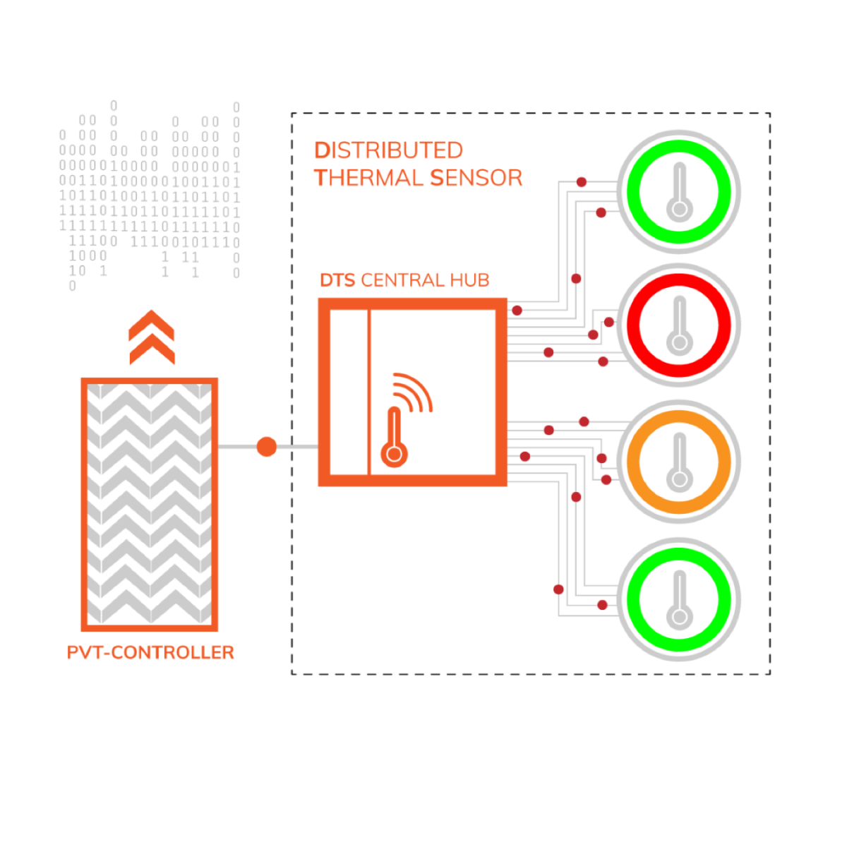
Of course, this means even more transistors on a chip. In turn, this has prompted the folks at Moortec to announce a new distributed temperature sensor (DTS) solution for use in the N6 and N5 nodes today and in future nodes tomorrow.
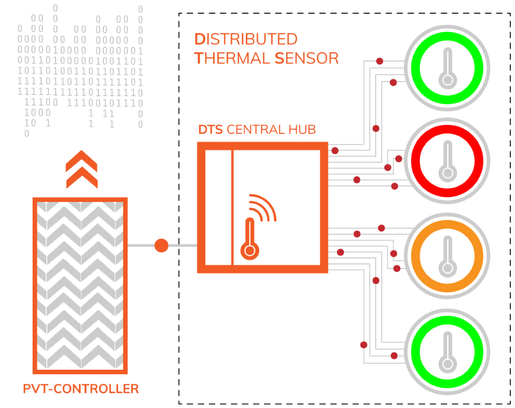
Moortec’s new DTS solution (Image source: Moortec)
Now, this is where things get tricky, but my understanding is that each DTS central hub will support 16 remote thermal sensors, plus an additional sensor in the hub itself. Meanwhile, the PVT controller can support up to eight DTS hubs and — just to add a dollop of cream onto the top of the cake — developers can employ multiple PVT controllers in their designs, if they wish.
The folks at Moortec tell me that the DTS is being licensed as an offering alongside their current (legacy) TS solutions. Developers will make a selection based on their applications, SoC architectures, and other specific performance requirements.
The new DTS possesses the same attributes as the traditional TS — robust to noise, high resolution, and highly accurate — but it is differentiated by the following:
- Smaller scale, having multiple remote sense points, thereby enabling a more granular, thermal mapping/profiling approach to sensing heat across the die.
- Integration is well suited to placement within large digital blocks or within individual CPU cores. The remote probes can also be located deep inside the chip’s core.
- Low latency, high speed sampling rate. Ideal for the “bursty activity” and variable workloads seen in the multi-core architectures used within high-performance computing (HPC) and artificial intelligence (AI) applications (for example).
These features will benefit developers by providing them with greater insight as to the activity of the chip, therefore enabling a greater opportunity to optimize performance and enhance reliability.
As usual, I’m left with my poor old noggin jam-packed with ideas ricocheting back and forth. We are already creating chips at the 6 nm and 5 nm technology nodes? These chips can contain tens of billions of transistors? Developers can now include temperature and voltage sensors throughout the chip and embed them deep within processor and accelerator cores? I’m too young for all this excitement!


https://physics.nist.gov/cgi-bin/cuu/Value?asil states that the silicon lattice constant is 0.5431 nM. Since there are eight silicon atoms in one unit cell, the spacing between atoms is about half this, or 0.27 nM. Thus 6 nM is about 22 atom spacings, 5 nM is about 19 atom spacings, and 3 nM is about 11 atom spacings. We are running out of atoms.
That’s not a problem — we’ll just use smaller atoms — you see, I’m a problem solver 🙂