

STMicroelectronics has added a new member to its line of VL53 FlightSense TOF (time of flight) distance/ranging sensors, but this new sensor takes a radical departure from the previous generation by replacing a conventional lensing system with metalenses, developed in conjunction with a startup company called Metalenz and based on technology originally developed in a Harvard University metamaterial lab. According to Metalenz, this is the first commercial product to incorporate its metalens technology.
Engineered metamaterials meet or exceed the capabilities of the conventional materials they replace by harnessing the properties of multiple-element arrays, where array elements are fabricated at scales that are smaller than the wavelengths of interest and arranged in repeating, mathematically placed patterns. For metalenses, that means patterning arrays of transparent dots on top of a semiconductor wafer to achieve lens-like properties using micro-diffractive optics.
ST’s TOF sensors determine distance to a target object by observing a photon’s time of flight from an emitter to the target, which then reflects the photon and sends it back to a receiver. ST doesn’t explain how its TOF sensors measure the photon’s back-and-forth time of flight, but it’s likely not a direct measurement. Light takes about 3.3 picoseconds to travel 1mm, so the sensor would need a pretty fast clock to count the individual picoseconds needed for the photon’s round trip between the sensor and an object.
There are ways of determining a photon’s time of flight using the observed phase shift between the output of a modulated light source and the return signal from the reflected light, and ST is likely using one of these techniques. Because these TOF sensors use SPAD (single-photon avalanche diode) arrays, I suspect it’s a digital modulation technique. Fortunately, you don’t need to know how ST’s TOF sensor works to use it in a design. You simply give the sensor some power and it provides you with a digital representation of the range to a target object.
Even before ST added metalenses into the technology mix for these TOF sensors, the VL53 sensor family integrated some pretty exotic electronics including an infrared VCSEL (vertical cavity surface-emitting laser) used as the photon emitter and arrays of SPADs used as photon receivers. In the previous generation of TOF sensors, both the VCSEL and SPAD array were topped with conventional lenses. For the company’s new VL53L8 sensor, both the VCSEL and SPAD arrays incorporate integrated metalenses fabricated on silicon by ST.
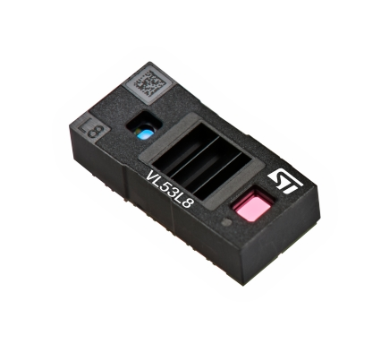
STMicroelectronics’ VL53L8 TOF sensor focuses light with flat metalenses instead of conventional lenses over the laser emitter and photoreceiver array.
The resulting TOF sensor can achieve more than double the range – as much as 4m in indoor settings – or it can operate at half the power consumption relative to ST’s previous generation of VL53 TOF sensors. The expanded range and reduced power consumption arise from a combination of a more efficient VCSEL driver circuit and the improved light-gathering ability of the metalens covering the SPAD array. ST’s announcement did not specify a minimum target distance for the VL53L8 sensor, but its predecessor, the VL53L5CX sensor, has a minimum ranging distance of 2cm and an apparent resolution of 1mm, with ±15mm accuracy in the 20-200mm range and 4-11% in the 201-4000mm range, depending on ambient lighting.
Like the earlier VL53L5CX sensor, the new VL53L8 sensor can determine distance to a target or multiple targets simultaneously using either 16 zones at 60Hz or 64 zones at 15Hz, as observed through a 43.5° x 43.5° square field of view. An integrated microcontroller in the TOF sensor delivers range-to-target information directly over an I2C or SPI serial interface and can generate interrupts to wake a host processor when each distance reading is made. Even with all it packs inside, this is a physically tiny sensor, measuring 6.4 x 3.0 x 1.75 mm. It’s supplied as a single, factory-aligned, reflowable component so you can drop it into a variety of products, even small portable ones.
The broad list of applications that can use TOF proximity sensing includes camera autofocus systems, robots and drones, touchless bathroom fixtures, and even automatic doors. It’s hard to tell if this technology is even a possibility for your next design without knowing roughly how much it costs. As is normal these days, ST’s press materials don’t include pricing, so I did a Google search and Mouser’s site came up. As of early June, the price for a reel of ST VL53L8CAV0GC/1 TOF sensors was listed as $22,464, and none were in stock. With 3600 devices per reel, the unit price works out to $6.24. That’s a pretty affordable sensor, especially considering all of the technology that’s packed into the device. If you don’t want 3600 devices, ST has a sampling program and makes these sensors available on evaluation boards.
Among several possible applications, the sensor’s multiple zones can be used for setting camera focus using a touch-to-focus user interface or to create a coarse depth map – a small point cloud. ST has developed demo applications including gesture tracking and liquid-level sensing for earlier sensors in the V53L family, and I’m guessing that work applies to the new VL53L8 sensor as well.
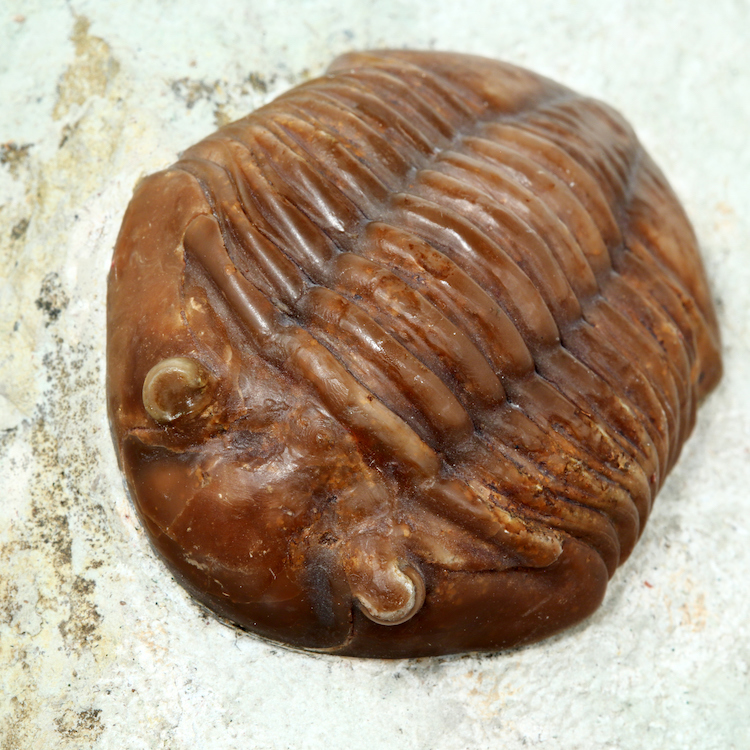
Although metalenses may seem like a cool new technology, they’re closely connected to something that’s quite old. As in hundreds of millions of years old. Some trilobites from the Cambrian Period had compound eyes with as many as 15,000 lenses. The fossil record strongly suggests that the trilobite’s eye could build a single coherent image from these thousands of smaller images, just as flies, shrimp, and lobsters do today. One trilobite species, dalmanitina socialis, had compound eyes with lenses consisting of two different, stacked lens units made from different materials. The larger, upper lens unit was made of calcite (calcium carbonate or CaCO3) and the lower lens unit was made of an organic compound.
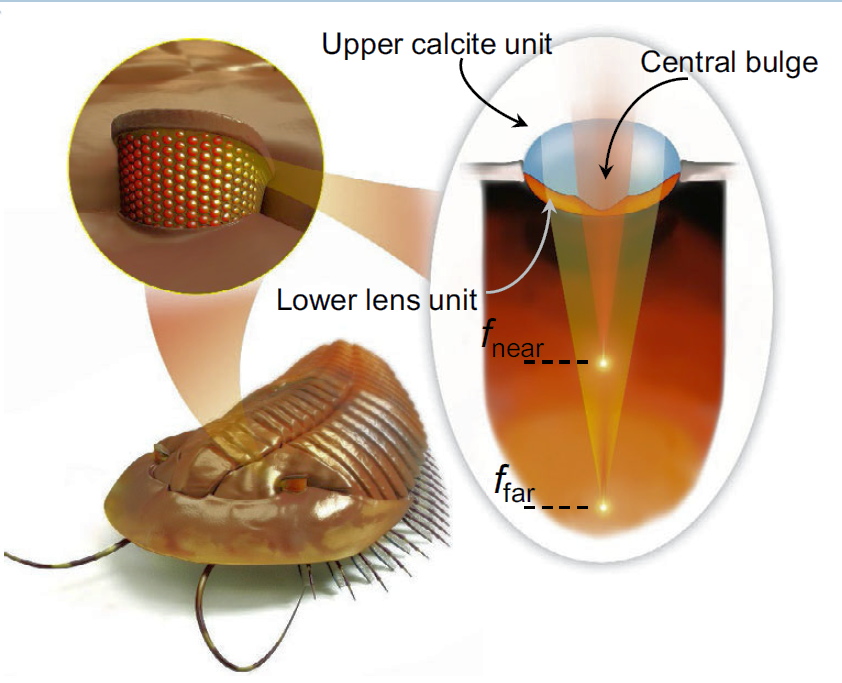
The compound eye of a dalmanitina socialis trilobite had thousands of lenses made of two different materials that allowed the eye to focus on close and far objects at the same time. Photo credit: NIST
Because they were made from different materials, the two lens units had different refractive indices and, therefore, each lens unit bent the incoming light differently and had a different focal point. As a result, each lens in this trilobite’s eye had simultaneous near and far points of focus.
Now I need to point out that there are some differences between the trilobite’s lens and a metalens. Trilobite eyes used conventional lenses, not metalenses, and Metalenz doesn’t use thin films of calcite or organic compounds to make its metalenses. (However, the company’s patents do mention several candidate oxides for metalens materials including silicon dioxide, which is extremely compatible with CMOS wafer processing.)
From the data sheet, it appears that ST’s VL53L8 TOF sensor is just using Metalenz’s metalenses as cheaper, better lenses to replace the classical bulk lenses that the company used for its previous TOF sensor generations. However, metalenses promise a lot more potential that needs to be explored.
For example, Metalenz has developed a technology called Gemini that merges two sets of metalenses in one array. Used with a VCSEL, one set of metalenses in the array projects laser light in a solid field. The other set projects lights as separate dots. The solid illumination, also called a flood fill, is better for close distance ranging, up to about 5m. Dot projection is better for more distant ranging, out to perhaps 10m. Metalenz’s Gemini technology allows you to select between the two projection patterns using an electronic signal, and, as a reminder: this technology is manufactured with low-cost semiconductor processes, so it’s relatively cheap, and there are no moving parts, so it’s rugged.
Based on the data sheet, it appears that ST isn’t using Gemini technology in the ST’s VL53L8 TOF sensor, but it certainly could use this capability as a range extender in future TOF sensors. In fact, Metalenz announced earlier this year that it is collaborating with Trumpf Photonic Components to develop switchable illumination modules based on Metalenz’s Gemini technology and Trumpf VCSELs.
That’s not the limit for metalenses; not even close. Just this year, researchers at the US National Institute of Standards and Technology (NIST) reported on a project that used a complex array of 39 x 39 metalens elements to project 1521 tiny images on a light-field camera’s sensor plane. Some of the images are focused on nearby objects, and others are focused on objects that are far away, and the camera assembles an overall image with nearly infinite depth of field from these smaller images. The NIST paper, titled “Trilobite-inspired neural nanophotonic light-field camera with extreme depth-of-field,” says that the project’s metalens images are similar to the lenses in the compound eyes of dalmanitina socialis.
A reconstruction algorithm based on a multiscale convolutional neural network assembles the final image from the 1521 small images and interpolates sharpness for intermediate distances, yielding a final image with a very large depth of field. Conventional photography employs a technique called focus stacking that builds a sharp image from several layered macro images, each taken with a slightly different focus point but with a very narrow depth of field. A software algorithm running on a computer then assembles a final image with much greater depth of field by merging the in-focus sections from the multiple images in the focus stack. In some ways, the NIST imager seems to be using a related concept, but on a much larger scale, with far more interpolation, and using parallel imaging.
Although the NIST research has created a light-field camera with immense depth of field, it’s not a TOF ranging sensor. The sensor used in the NIST research is a conventional image sensor, not a SPAD array. Most TOF sensors incorporate very small SPAD arrays that are too coarse for useful imaging. For example, ST’s new VL53L8 sensor has only 64 elements in its SPAD array, which is not even close to the current record for SPAD array sensors.
Late last year, Canon announced that it had developed a 3.2-megapixel SPAD sensor, and the accompanying press release expressed “expectations that this technology may be used to obtain high-speed, high-precision 3D information for such applications as distance measurement for automated vehicles, Augmented Reality (AR) and Mixed Reality (MR).” The same press release says that Canon will start producing these large SPAD image sensors for use in the company’s security-oriented network camera products later this year.
Based on these developments, I sense (pun intended) there’s a real revolution brewing for electro-optical imaging. I can’t wait to see the results of the fermentation process. It’s only taken a few hundred million years to get here.


