

It’s not often that I have the chance to introduce a new field-programmable gate array (FPGA) family, and even rarer that we get to greet a new FPGA vendor, so my cup runneth over because Renesas Electronics Corporation just leaped into the FPGA market with the announcement of a new line of very low-cost, very low-power, very interesting ForgeFPGA devices.
Before we focus on ForgeFPGAs, let’s first set the scene by considering their ancestry and contemplating how we came to find ourselves in this place at this time. This all started with a company called Silego Technology Inc., which was an independent Silicon Valley-based fabless semiconductor company until it was acquired by Dialog Semiconductor in November 2017. Of course, Dialog was itself acquired by Renesas in August 2021, which was around three months ago as I pen these words.
Prior to its acquisition by Dialog, Silego created a dynasty of disparate devices, but its real claim to fame was a series of GreenPAK (GPAK) chips. I think of these little beauties as being teeny-tiny mixed-signal FPGAs, but the chaps and chapesses at Silego / Dialog / Renesas prefer to refer to them as configurable mixed-signal ICs (CMICs). These GPAK CMIC components are ultra-small with respect to size, ultra-low with respect to power consumption, and ultra-affordable with respect to cost (they are only pennies a piece in bulk).
Silego was ranked as the second fastest growing semiconductor company in North America at the 2011 Deloitte Technology Fast 500 event held in Menlo Park, California. By August 2016, Silego had shipped more than 2 billion CMICs, which is not a number to be sneezed at (especially when you realize that sneezing is a good way to disperse these miniscule devices over a wide area).
It really is worth taking a moment to consider GPAK devices and design tools in a little detail, because this will help us to wrap our brains around their ForgeFPGA cousins. The first GPAK device I used myself was the GPAK4, which supports a supply voltage of 1.8V to 5.0V, and which is presented in a 20-pin STQFN 2.0 x 3.0 x 0.55 mm package with a 0.4 mm pitch.
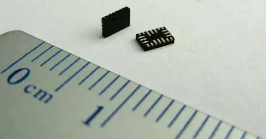
A GPAK4 CMIC.
This little rascal boasts 18 general-purpose input/outputs (GPIOs), 6 analog comparators, 3 digital comparators/pulse-width modulators, 2 digital-to-analog converters, 25 look-up tables (LUTs), and a variety of counter, delay, and flip-flop macrocells.
One really cool thing about GPAK devices is that they employ RAM configuration cells that can be programmed over and over again while you are in the process of developing your design. Once you are ready for deployment, you can transfer your design into the chip’s one-time programmable (OTP) non-volatile memory (NVM). After you’ve programmed the NVM, on power-up, the device will automatically copy the configuration from the NVM into the RAM configuration cells, and off we go.
The GPAK4 was followed (not surprisingly) by the GPAK5, which is presented in the same package. This clever little scamp augments the GPAK4’s features and functions with the addition of an asynchronous state machine (ASM) block, an 8 x 8 scratchpad memory, and an I2C block. The ASM has been described as providing equivalent functionality to a simple microcontroller running around 100 lines of code. Meanwhile, the I2C block can be used to reconfigure the contents of the RAM (selected bits or the whole kit and caboodle) after the device has been powered up, which can be useful for tasks like tweaking analog comparator threshold settings or modifying time delay values under the control of some higher-level system.
One of the things that impresses me most about this whole setup is the free design and development tools, starting with an intuitive, easy-to-use, drag-and-drop graphical user interface (GUI) called GreenPAK Designer that allows you to select the components, configure them, and connect them to each other and to the device’s primary inputs and outputs.
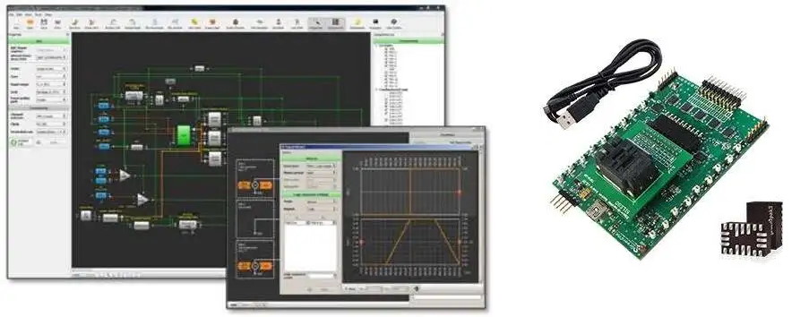
GreenPAK Designer (left) and the GreenPAK Development Kit (Right)
Also included is a waveform editor with an associated wizard that allows you to describe sophisticated analog and digital stimulus waveforms. You can use GreenPAK Designer to simulate your design on your host computer. When you are ready to rock-and-roll, you can download the design into your GPAK chip located in a zero-insertion-force (ZIF) socket mounted on top of the GreenPAK Development Kit, and then reverify your design in the real-world device (as discussed earlier, you can load the design directly into the chip’s RAM configuration cells, or you can load it into the OTP NVM).
OK, now that we’ve set the scene, let’s return to the main topic of our conversation, which is the announcement of Renesas’s new ForgeFPGA family.
I was just chatting with my old chum Nathan John, who has been instrumental in guiding all of these technologies since the Silego days. Nathen tells me that ForgeFPGAs are the next logical progression from GPAK CMICs because customers have long been saying that they love the features and functionalities of the CMICs, but they want more, more, more (bless their little cotton socks).
The result is the ForgeFPGA family, which addresses the underserved market need for relatively small amounts of programmable logic that can be quickly and efficiently designed and deployed into cost-sensitive applications.

Meet the first member of the ForgeFPGA family.
What we are talking about here is applications that require less than 5,000 equivalent logic gates with a projected price in volume of “well under $0.50 in US dollars.” Initial ForgeFPGA offerings will be purely digital with device sizes of 1K and 2K LUTs, but I wouldn’t be surprised to see GPAK-like analog functionality appearing in the future.
As with the GPAK devices, users will be able to download the ForgeFPGA development software, which is called ForgeFPGA Workshop, at no cost and with no license fees. This new incarnation of the software now includes two design capture modes as illustrated below:
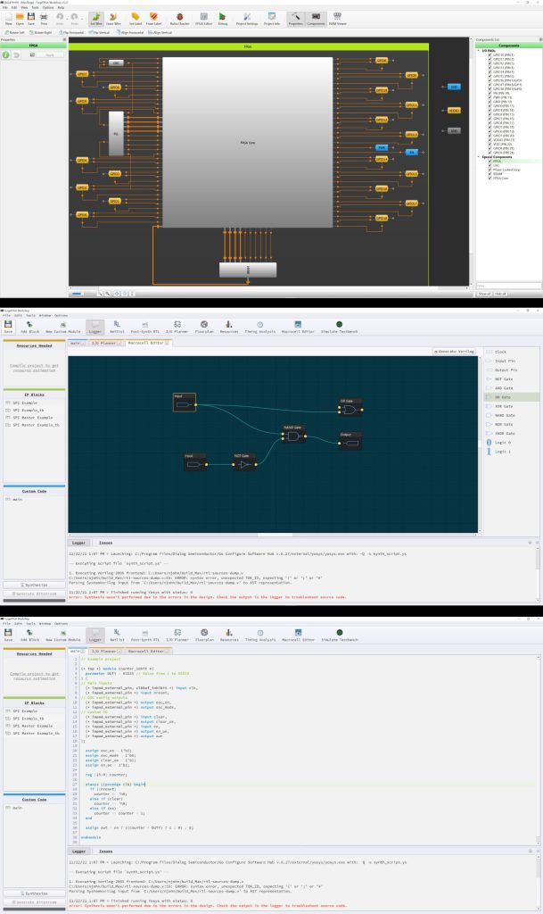
ForgeFPGA Workshop; Default view (top), Macrocell mode (middle),
and HDL mode (bottom).
We start with the main GUI, which presents a graphical view of the GPIOs surrounding an area annotated as being the “FPGA Core,” which represents the programmable fabric. At this point, the user has two options: for newcomers to the FPGA world there’s a “macrocell mode” that uses a schematic capture-based development flow similar to the original GPAK drag-and-drop interface; for designers with more FPGA experience there’s an “HDL mode” that provides a familiar Verilog environment. Also, there’s an associated hardware development kit.
ForgeFPGA engineering samples are available now, along with beta design software and a prototype development kit. The first ForgeFPGA device, the 1K LUT offering, which is presented in a 3 x 3 mm package, is expected to be available in production quantities in Q2 2022 (click here if you want to learn more).
I must admit that I’m rather excited to see Renesas enter the FPGA market, but what does everyone else think about this news? Well, my chum and co-writer here on EEJournal — Steve Leibson — recently donned his hat as Principal Analyst at TIRIAS Research to say:
Having scooped up programmable device maker Silego with its acquisition of Dialog earlier this year, Renesas seems determined to repeat Silego’s previous success with its ultra-low-end GreenPAK line of programmable mixed-signal devices and super-simple design tools, this time in a low-end FPGA line that will appeal to many companies who just need a bit of programmable logic — a thousand gates or so — to get the job done in myriad products including billions of embedded sensors and IoT devices.
I couldn’t have said it better myself. How about you? What do you think about all of this? As always, I welcome your sage comments and insightful questions.


Hi Max! Hope you are well. A few details we’re all wondering about:
1) Does this baby have an SPI interface for host micro to load new configuration into NVRAM? Or what?
2) VHDL, verilog, both, other?
3) Price/function comparison with low-end Lattice parts?
Thanks Max!
See ya, Dave
Hi Dave — awesome questions — re (2) I do know that it’s currently Verilog only. Re (1) and (3), I’m going to ask my chum Nathan John at Silego / Dialog / Renesas if he can respond to your questions (or tell me the answers so I can respond).
Regards — Max (1/2 man, 1/2 beast, 1/2 wit)
Dave,
In answer to your questions:
1) Does this baby have an SPI interface for host micro to load new configuration into NVRAM? Or what?
Answer 1: The active registers on the parts in this family are SRAM based. The user has the option to load these registers from internal NVM (OTP for the first device), or to load from external via SPI in master mode or slave mode
2) VHDL, verilog, both, other?
Answer 2: Initially Verilog, future update to include VHDL support.
3) Price/function comparison with low-end Lattice parts?
Answer 3: We plan to make these parts very attractive from a pricing standpoint.
Link for Software Download:
https://www.dialog-semiconductor.com/go-configure-software-hub
Nathan John
Renesas
I’ve played with GreenPAK devices. They’re pretty awesome, though a bit to analog-y for me. This however is pretty awesome. Too bad it’s not on the market yet … And too bad VHDL is not yet supported. We lov… err … use it a lot here in Europe 🙂
That’s funny because I’m looking forward to them adding the GPAK analog bits back into these FPGAs 🙂
As to VHDL — on the one hand… but then, on the other hand… LOL