


There’s a famous saying along the lines of, “Predicting things is difficult, especially about the future.” This quote has been attributed to many people, including Mark Twain, Niels Bohr, and Yogi Berra. In Yogi’s case, however, it’s usually phrased as, “It’s tough to make predictions, especially about the future.”
I know that when I staggered into the current millennium, buoyed by the Y2K celebrations, I would never have predicted the current surge into multi-die system space (where no one can hear you scream).
Let’s briefly set the scene to ensure we’re all tap-dancing to the same skirl of the bagpipes. According to an article by Brian Santo on EETimes, the term “chiplet” can be found in patents as early as 1969. However, this referred to column driver chiplets attached to large LCD panels. The use of “chiplet” in the context we understand today was coined by University of California, Berkeley professor John Wawrzynek in 2006 (OMG, that’s almost 20 years ago as I pen these words).
As recently as five years ago, in 2020, the topic of chiplets wasn’t heard often in mainstream usage. Now, by comparison, one cannot help but hear people talk about it (the trick is to get them to stop talking about it).
Chiplets mean different things to different people. In my earlier Are You Ready for the Chiplet Age? column from 2023, I noted that Synopsys had identified four main chiplet use cases. As I said back then:
The first scenario is to simply scale things by mounting multiple homogeneous dice (think processors like CPUs, GPUs, NPUs, etc.) on the same substrate.
The second is to take a design that you would ideally like to implement in the form of a humongous monolithic die and split it into two or more smaller chiplets.
The third is based on the fact that input/output (I/O) functions like transceivers and memory interfaces typically don’t benefit from being implemented at the latest and greatest technology node. In this case, the best solution is to create the main die containing your “secret squirrel (logic) sauce” at the latest technology node, and to realize your high-speed interfaces as proven, risk-free chiplets implemented at an older process technology (some people refer to this as “N – 2 nodes”).
Last, but certainly not least, the fourth scenario involves disaggregating everything into heterogeneous dice implemented at the best nodes (in terms of cost, power, etc.) for those functions. For example, an RF die implemented using a 28nm process, analog-to-digital converters (ADCs) implemented in a 16nm process, and digital logic implemented in a 5nm process.
The way we typically design ASICs and system-on-chip (SoC) devices today is to purchase off-the-shelf intellectual property (IP) blocks from trusted third-party vendors. These “soft IPs,” which are presented in the form of register transfer level (RTL) files, cover things like processors, on-chip memory blocks, and DDR controllers. The designers also create their own “secret sauce” accelerator IPs that (they hope) will differentiate their solution from those of their competitors. Then all the soft IPs are synthesized, integrated, and implemented on a single silicon die.
The equivalent chiplet-based vision for the future (which may be closer than we think) is that the designers of multi-die systems will essentially purchase off-the-shelf “hard IPs” in the form of chiplets from trusted third-party vendors. The designers will also create their own “secret sauce” chiplets. Then all these chiplets will be integrated on a common substrate (organic or semiconductor), which will be packaged and presented as a multi-die system.
We aren’t there yet, although we are seeing a lot of activity and interest in this area. So, what are we seeing on the chiplet front today, and what do we expect to see tomorrow? When it comes to chiplets, the place to “see and be seen” is the Chiplet Summit. The 2025 event took place just a couple of weeks ago (21–23 January) at the time of this writing. I was just chatting with Abhijeet Chakraborty, who gave one of the keynote presentations at the summit. Abhijeet is VP of Engineering and responsible for multi-die solutions at Synopsys.
Abhijeet kindly gave me an overview of his Chiplet Summit keynote, but I’m going to cover only a few items here. He started out by noting that what we are seeing today is that the increasing adoption of chiplets is predominantly driven by the demand for artificial intelligence (AI) chips.
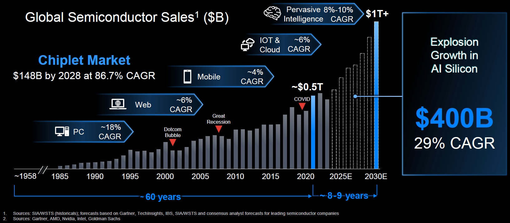
The increasing adoption of chiplets is driven by demand for AI chips (Source: Synopsys)
The slide above reflects the fact that the global semiconductor revenue is currently a tad over half a trillion dollars, and that it’s taken us about 60 years to get here. Growth drivers in the past have included the PC revolution with a compound annual growth rate (GAGR) of ~18%, the web and internet boom with a CAGR of ~6%, mobile devices with a CAGR of ~4%, and—more recently—the IoT and the cloud with a CAGR of ~6%.
Today, we are talking about the growth of pervasive intelligence with an expected CAGR of 8% to 10%. Although it took us 6 decades to reach a global semiconductor revenue of ~0.5 trillion dollars, it’s going to take us less than a decade to grow another 0.5 trillion to reach 1+ trillion dollars.
AI chips, both at the data centers and at the edge, are driving a lot of this growth, and we expect this growth to continue. In fact, the expectation is that by the 2028 timeframe, in just 3 short years, the AI Silicon market itself is going to be around 400 billion dollars with a very high double-digit CAGR. Eeek (and I mean that most sincerely)!
Currently, most multi-die system deployments come from the big players, like AMD, NVIDIA, and Intel. By definition, the smallest number of dice that qualify as a “multi-die” system would be 2. An example is NVIDIA’s Blackwell GPR with two multi-core GPUs. Each Blackwell GPU is comprised of two reticle-limited dice connected by a 10 terabytes-per-second (TBps) chip-to-chip interconnect, forming a unified single GPU. This design allows for a total of 208 billion transistors, with each die contributing 104 billion transistors. By comparison, AMD’s Instinct MI300 contains 8 multi-core GPU chiplets and 3 multi-core CPU chiplets along with multiple input/output (I/O) chiplets (the number of chiplets varies by variant, as it were).
STOP! Did you see the “10 terabytes per second (TBps) chip-to-chip interconnect” and the “208 billion transistors” in the preceding paragraph? You did? Oh, well, that’s alright then. I just didn’t want you to miss anything (I’m still suffering from heart palpitations thinking about these numbers).
Now consider the following graphic. Remember that this information comes from multiple sources, each having their own take on things. For example, the guys and gals at IDTechEx predict that the entire chiplet market will be 411 billion dollars by 2035, with servers and cloud computing accounting for more than 50%.

Predicting a rapid adoption of multi-die designs (Source: Synopsys)
By comparison, when focusing on a subset of distinct chiplets, the chaps and chapesses at Market.us predict a market of 107 billion dollars by 2033 with a CAGR of 42.57% (which I personally would have rounded to ~43% because “42.57%” seems to be a little too precise).
Our chat ranged far and wide, but I’m going to jump to the end when Abhijeet presented his projections and predictions for 2025. These predictions are summarized below.

Predictions for multi-die systems in 2025 (Source: Synopsys)
Abhijeet says the folk at Synopsys are estimating that at least half of new chip designs in the high-performance computing (HPC) market will be multi-die (they consider AI to fall under the HPC umbrella).
With respect to “3D multi-die designs,” this refers to stacking dice on top of each other. We’re not talking about homogeneous stacks of memory dice like we see in high-bandwidth memory (HMB); instead, we’re talking about stacking heterogeneous dice on top of each other, thereby minimizing the lengths of signal paths while reducing latency and power. Abhijeet says that the folks at Synopsis are at the forefront of the field because they are working with leading-edge customers in this space: developing solutions, solving problems, and collaboratively creating reference flows.
On the manufacturing side, Abhijeet says that he and his colleagues expect increased foundry capacity, thanks in large part to the increased focus from the US government (including the US Chips Act) and other governments around the world. Also, more advanced package types and technologies are coming online.
Last, but not least, we have technology maturity in terms of EDA and IP solutions targeted at multi-die designs, including 3D die-stack implementations.
All I can say is that it’s clear that multi-die system designs are no longer a futuristic concept but an industry-shaping reality. The rapid adoption of chiplets, fueled by the insatiable demand for AI and HPC, is transforming the semiconductor landscape at an unprecedented pace.
In the case of data centers and cloud computing, the days of monolithic ASICs and SoCs dominating the field are fading. In their place, we are witnessing the beginning of a new era—one where modularity, flexibility, and heterogeneous integration define the cutting edge. The figures are staggering, the growth projections eye-watering, and the engineering challenges formidable, but the momentum is undeniable.
The pioneers of this revolution—AMD, NVIDIA, Intel, and others—are proving what’s possible. But as manufacturing capabilities expand, advanced packaging technologies mature, and EDA solutions evolve, the multi-die paradigm will become more accessible to a broader range of innovators. Before long, today’s industry giants will find themselves competing with a new wave of challengers, empowered by an ecosystem of off-the-shelf chiplets and customizable multi-die solutions.
To cut a long story short (which isn’t the way I usually like to do things), multi-die design isn’t just a trend—it’s the future. And in a world driven by the relentless pursuit of performance, efficiency, and scalability, that future is arriving faster than we ever imagined. Buckle up, because the next few years are going to be one a heck of a ride!


One thought on “Predictions for Multi-Die System Designs in 2025”