


When I first started working for an FPGA company a decade ago, I was stunned to find out how many power supply rails these parts required. I’d never encountered chips that needed five to ten (or more) power supply rails. Even back in the old, old PMOS days, chips needed only three supply voltages and, for a few fortunate decades, 5 volts was all you ever needed for a power supply. Somehow, someone gave permission to FPGA designers to go hog wild with their over-the-top power supply requirements. This unhappy characteristic isn’t unique to one vendor’s FPGAs. These days, nearly all FPGAs except for the oldest and simplest are like that.
For years, FPGA vendors have worked with power-management IC (PMIC) chipmakers to develop power subsystem reference designs that deliver all the myriad required power rails for their FPGAs. You may have noticed that there’s a tendency for FPGA vendors to prefer PMIC vendors that share the same electronics component distributor with the FPGA vendor, so chances are good that if you prefer an FPGA from one vendor, and most engineers have taken sides in the FPGA wars thanks to EDA tool lock-in, you might not find a power subsystem reference design for that FPGA based on a chip from your preferred PMIC vendor. If you use FPGAs from multiple vendors, you might not be able to use the same PMICs to power the different brands of FPGAs, at least not using the vendors’ reference designs. You might need to design your own power subsystems or ask your favorite PMIC vendor to design something for you.
Now, there’s another alternative. It comes from a somewhat obscure programmable analog semiconductor company called AnDAPT. (Yes indeed, that’s how the company capitalizes its name.) AnDAPT was founded by Kapil Shankar, who previously founded and was CEO of FPGA vendor SiliconBlue. (Shankar apparently likes company names with weird capitalizations.) Lattice Semiconductor eventually bought SiliconBlue, and Shankar’s new venture, AnDAPT, is focused on programmable analog ICs.
Though they’re rare, AnDAPT is not the first programmable analog device company I’ve encountered. The first company that I can recall taking a stab at programmable analog parts was International Microelectronics Products (IMP) in San Jose, California. That company’s electrically programmable analog circuits (EPACs) – billed as “analog FPGAs” – tried to replace jellybean analog semiconductors like op amps and comparators, and discrete passive devices including resistors and capacitors, with programmable semiconductors.
There’s not much information on the Web about IMP because the company went bust just before the Internet exploded. However, I did find an incidental remark about IMP made by David Laws – who worked as VP of Marketing at Altera in the early days, as President of QuickLogic for four years, and who consulted for the semiconductor industry for decades – during a 2012 panel discussion about AMD’s development of the 22V10 PAL that he moderated for the Computer History Museum:
“I consulted with IMP on a programmable analog device. They could build a neat, customized op amp for about five dollars. Unfortunately, with off-the-shelf devices selling for 10 cents, it didn’t go very far. But it was an interesting technological exercise.”
Most MBAs will tell you that an “interesting technological exercise” is not a great foundation for building a financially successful company and, as David Laws explains in a separate oral history with Stanford University’s Silicon Genesis project, people loved the EPACs, but not enough people bought them in volume. IMP continued as a specialty foundry, got bought, and eventually went out of business.
Based on that history, AnDAPT might have an uphill battle on its hands. But I think the company may have found just the right niche for achieving some success: powering FPGAs from the major FPGA vendors. AnDAPT’s Adaptive Multi-Rail Power Platform (AmP) PMICs are SRAM-based, programmable power devices that seem like just the ticket for generating numerous FPGA supply rails. AmP PMICs incorporate programmable power-switching and linear regulators as well as analog comparators, amplifiers, and power FETs in their programmable analog fabric. They also include some amount of programmable logic in a digital fabric that includes the more familiar LUTs and RAMs, which are used for making decisions and sequencing.
As mentioned above, modern FPGAs require multiple supply rails. Some of these rails must supply high currents – tens of amps – and some require relatively low currents. The high-current supply rails are generally implemented as switching power supplies, for efficiency, and the low-current rails generally employ linear pass regulators, for lower cost and simplicity. So, there’s a mix of voltages and supply currents to deal with when designing a power subsystem for an FPGA.
For example, here’s the power supply map required by an AMD-Xilinx Zynq UltraScale+ MPSoC, an SoC that combines an FPGA with a processor-based SoC:
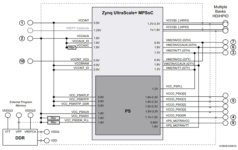
As the graphic shows, the Zynq UltraScale+ MPSoC requires ten unique supply rails, shown as numbered bubbles 1 through 10. However, the complexity associated with supplying power to a device like the Zynq UltraScale+ MPSoC goes beyond the voltages and currents required. The power rails must be initialized in the proper sequence and with the proper timing when the system powers up and may also need to be properly sequenced when the power shuts off, as well. Violating power rail sequencing and timing specifications can destroy these kinds of devices. That means designing power subsystems for these types of devices is partly an analog exercise and partly a digital one.
To be fair, all FPGA vendors realize the kind of power supply design challenges they’ve dropped into the laps of system developers who want to use an FPGA, and they have worked with PMIC vendors to develop canned power supply subsystem designs that meet the requirements of their programmable logic devices. According to AnDAPT’s CEO Bill McLean, the FPGA vendors have done a pretty good job of developing PMIC-based solutions for power subsystems running from 5-volt intermediate power rails.
However, some FPGA-based systems designs use 12-volt intermediate power rails and AnDAPT has discovered that this niche is not well served by existing PMIC-based solutions. The company has decided that it wants to stake its claim on this 12-volt niche. To that end, AnDAPT has developed canned power subsystem designs for a growing number of programmable logic devices from AMD-Xilinx and Microchip.
For example, the company has designed a two-chip power subsystem design for the Zynq UltraScale+ MPSoC that’s based on the company’s AmP ICs, as shown in the table below:
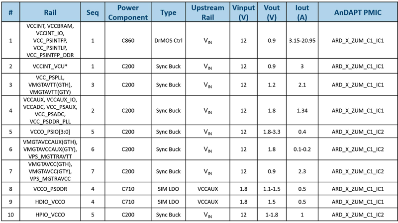
Both AmP PMICs used for this power subsystem design, labeled ARD_X_ZUM_C1_IC1 and ARD_X_ZUM_C1_IC2 in the table’s last column, are the same basic AmP device, but they have been programmed differently to generate different supply rails. PMIC configuration occurs during power up, just like other SRAM-based programmable-logic devices. AmP PMICs load their configuration over a SPI (serial peripheral interface) port, either acting as a SPI master and loading the configuration bitstream from a serial EEPROM or acting as an SPI slave and accepting a configuration bitstream from an external controller. (Note: If you are offended by the use of SPI master/slave notation, I apologize and empathize, but those are the official names of the SPI standard.)
What the table above does not show is that these AmP PMIC-based power subsystem designs also require external inductors, capacitors, and diodes. However, you expect that because those power components are not easily integrated into a chip. It’s much the same when using most PMICs from other vendors. AnDAPT’s canned power subsystem designs and its design tools provide specifications for these external components as part of the downloadable design file package that the tools generate.
To carve out this 12-volt niche, AnDAPT has developed reference power subsystem designs for several AMD-Xilinx and Microchip FPGAs. AMD-Xilinx FPGAs covered include the Zynq UltraScale+ MPSoC and RFSoC families, and the original Zynq-7000 SoC family; the Kintex UltraScale+, UltraScale, and Kintex-7 FPGA families; and the Artix UltraScale+ and Artix-7 FPGA families. The company has plans to develop designs for the AMD-Xilinx Virtex and Spartan-7 FPGA families and Versal ACAP families later this year. AnDAPT has also developed reference designs for Microchip PolarFire FPGAs.
You can modify these power subsystem designs or create your own design from scratch using AnDAPT’s Web-based EDA tools. These tools employ a simple, graphical, drag-and-drop user interface, and, based on the demonstration videos I watched on the AnDAPT Website, you can probably design a power subsystem with these tools in less time than it takes to eat lunch, and without knowing Verilog or VHDL.
So, if your designs include the need for several precision power subsystems running from 12-volt intermediate supply rails, and you don’t have a solution handy, you might want to give AnDAPT’s AmP PMICs a look.
References:
“Interview with David Laws, 2013 June 07,” Silicon Genesis, Oral Histories of Semiconductor Technology, Stanford University


Hi Steve, Regarding “I was stunned to find out how many power supply rails these parts required.” Agreed, I also was stunned to see FPGA design engineers adding rails to make the FPGA cheaper, or faster, without any regard to increasing complexity beyond the chip.
Regarding “Shankar apparently likes company names with weird capitalizations.”, I must admit, I am somewhat complicit in weird capitalizations with previous names such as AmP, WebAmP, AmPLink, AmPScope, SiliconBlue, mobileFPGA, iCE65, QuickLogic, pASIC, ViaLink, PAL, PALASM, SkinnyDIP. 🙂