


Today we wander back into the field of silicon photonics. A few years ago, I did a quick summary of how light can be manipulated in silicon, and, shortly thereafter, I did a review of some of the conceptual issues surrounding design tools and automation.
This year at DAC, however, I talked with Mentor regarding their use of the Calibre DRC tool for photonics, and that led to a conversation with PhoeniX, makers of photonics design tools – which can use Calibre in the verification flow. This lets us get much more specific than we did in the earlier piece.
It’s fair to say that photonics design has been pretty old-school, with a methodology involving the manual creation of shapes. (Thankfully, no rubylith.) This is changing, but, to a large extent, we have not yet seen the type of abstraction that has characterized digital design, boosting productivity to ridiculous levels. Although, as we’ll see, perhaps it’s only a matter of time.
Photonics design can also involve a variety of tools. High-level functionality in Matlab; lots of simulations – S-matrix in one tool, time domain in another tool. Mentor is trying to bring some of this together in a high-level cockpit through their Tanner group, but there’s more to be done.
Mentor summarizes the flow from their vantage-point in the image below. You’ll notice that PhoeniX handles much of the original design work, plugging into the Design Cockpit. But this focuses on the Calibre contribution, so we should also dig into what PhoeniX OptoDesigner brings to the party. It bears noting that, per the older design article linked above, there are other tools used for photonics design. My focus on PhoeniX is based on their integration with Mentor’s tools.
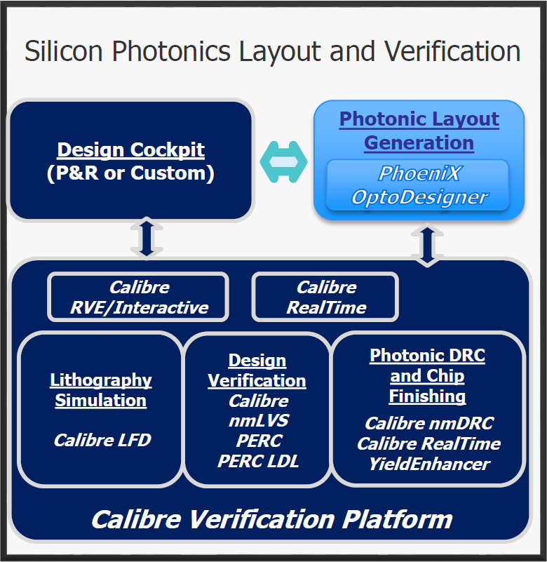
(Image courtesy Mentor)
Photonics Design. Old School
At its most basic level, photonics design has you drawing what you want and then doing lots of simulations to tweak it into shape. There are different types of simulation, but “lots” also refers to an iterative process.
Two of the main simulation types are “mode” solvers and “propagation” solvers. The former is performed on a cross-section of the optical waveguide, where modes will be evident. Refractive indices are the prime determiners of those modes, but you can also include the effects of electrical fields, temperature, and mechanical stress.
Propagation, by contrast, uses a top view and deals with how the light gets from point A to point B. There are many different algorithms that can be applied here, depending on the specifics of what’s being simulated. In some cases, it might be obvious which to use; in others, you may require some trial-and-error.
Modernizing the Flow
Building upon this fundamental flow are a number of recent and evolving changes that will make photonics design more productive. The first came about a decade ago, with the availability of process design kits (PDKs). PhoeniX says they were the first to include these, making layout less dependent on manual process targeting and helping to bend the optical flow towards circuit flows.
They’ve also added a process viewer, similar to what we’ve seen from Coventor and Synopsys, although it’s a 2D visualization, making it faster, if less “complete.” Cross-sections from this tool can be fed into the mode solver tool, making it unnecessary to draw the cross-section manually.
Next comes a big one: a start at synthesis. Here you specify your intent and the tool will generate a correct-by-construction, manufacturable (per the PDK) layout. Intent is expressed through a few statements that describe an optical function.
PhoeniX’s Mitch Heins described the synthesis operation as consisting of four steps – analogous to digital logic synthesis:
- Map from language constructs to technology-agnostic building blocks.
- Map from technology-agnostic building blocks to technology-specific building blocks
- Optimization of logic to reduce area and impact timing
- Layout and final optimization.
They currently implement steps 2-4. The building-block list as provided by Mr. Heins includes components like:
- Waveguides
- Somewhat equivalent to wires in electronics but with more impact on signal than wires
- Variants on waveguides for different corning types, tapering, etc.
- Splitters
- Directional Couplers
- Gratings (vertical couplers)
- Phase shifters
- Delay elements
- Photo detectors
- Modulators (multiple variants of each of the below)
- Amplitude
- Phase
- Polarity
- Multiplexers / De-multiplexers
- In photonics you can have multiple signals traveling down the same waveguide at the same time using different frequencies or colors. Mux/DeMux can add or drop different frequencies to/from the waveguide
- LASERs (light sources of varying types)
Step 1 in the synthesis flow involves higher-level architectural considerations of what components to use for a particular function. An example he gives is of a filter: should it be implemented using so-called Mach-Zehnder Interferometers (MZIs) or from micro-rings? The choice matters, depending on which parameters you’re trying to optimize. They see this as a work in progress and that software should be able to pick up this role. But for now, it’s still largely manual.
Working at a behavioral level lets you focus on higher-level functional simulation rather than the low-level layout simulation. It also increases the complexity of circuits that can be designed, since the number of simulations currently required can limit block size to some hundreds of components.
At the higher level, S-matrix simulation can be done natively within OptoDesigner. PhoeniX collaborates with other tools for time-domain simulation.
Getting Physical
Up to this point, the design tools carry a fully analytical description of the design. But now the idealized layout, with perfect curves – anathema to standard EDA tools – must be rendered in a manner that allows masks to be created. Here we transition from the optical flow into something more resembling an electrical flow.
The first step involves discretizing the shapes, a step that’s done automatically. The format for mask shapes requires “Manhattan” geometries: straight lines going vertically or horizontally. That means creating a piecewise linear approximation of any features that don’t resemble Manhattan.
What’s interesting about this is that this process works better on older nodes than newer nodes – specifically because the resolution is poorer, allowing these linear jogs to fuzz into curves. The length of the lines are depends on the grid imposed on the design; a finer grid creates more lines, but shorter ones. They say that the grid you choose can apply to any process node – it’s not determined by the resolution of any particular node.
After discretization, it’s time to do a layout check to make sure rules haven’t been broken. OptoDesigner has their own native DRC tool, but, because Calibre is something of a gold standard, they found that customers wanted a hook into that tool, which Mentor and PhoeniX have built. (Note that OptoDesigner also has various levels of integration with other non-Mentor tools as well.)
But there’s a problem: the piecewise linear onslaught can result in numerous false errors being reported. So Mentor uses eqDRC, which relies on equations rather than rules. This provides a much cleaner check, as shown by the following image they provided.
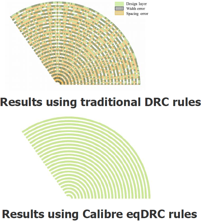
(Image courtesy Mentor)
Calibre’s SmartFill feature, which creates fill patterns in areas with little metal, also handles photonics differently so that the fill features don’t inadvertently interfere with the optical fields.
On the To-Do List
There are, of course, many more things to be done. Mentor had a list of items that are being worked:
- How to do device extraction
- Multi-physics simulations
- Moving from 130 nm to 65 nm
- Adding fill to older nodes (for shielding)
- Changing litho simulations from operating on as-drawn features to as-printed features
- Figuring out whether current simulations, based on computationally intensive finite-element analysis, will scale sufficiently as photonics circuits grow
Increased automation is also a goal; right now, it lies somewhere between digital circuits and analog circuits. One challenge with automating analog design lies in giving analog-design engineers confidence that the tools can do as good a job – or better – than they could do themselves. According to PhoeniX, photonics designers are not expressing the same reservations as analog designers, so automation (if well designed) should be welcome.
More info:


What do you think of the differences between silicon photonics and silicon electronics design tools?