


Several weeks ago we took a look at the expanding role of EDA. And then a couple weeks ago we delved into the bizarre world of silicon photonics. Yeah, we didn’t get too deep because the bottom drops off pretty quickly, and I’m not sure I could tread water credibly any deeper. But we got a flavor.
So now, we bring these two things together to answer the question, “If I’m going to be involved in a photonic chip design, what tools am I going to use?” OK, so if you’re an electronics designer, you’ll probably be asking the question, “What tools will the photonics pholks be using, and how will thier world interface to mine?”
Folks have been doing silicon photonics research for a long time now, and you need tools to do that. So it’s not like we’re just now seeing the emergence of new tools for this purpose. The thing is, there’s not a lot of profit in research, so the big guys that are commercially driven may not be attracted to such new endeavors in the early stages.
In fact, the way this usually plays out is that, early on, a few people with specialized knowledge in the area will labor away, getting tools to work. The fruits of their efforts may not be as spiffy in some ways as full-on commercial tools, but there’s also less of a time-to-market demand. So the focus is more on the kinds of calculations that are hard (or unrealistic) to do by hand, even though the design flow itself might take a bit more scripting and futzing about to get working.
But at some point, as a technology approaches its mainstream debut, other people start taking notice. And the easy way for mainstream tool vendors to get involved quickly is for a big company with deep pockets to find one of these small pioneers that seems to have done a good job and simply buy them. And, presto! You’re in the photonics business. Or you can partner up without an actual handfasting (casual relationships being so much more acceptable these days, ecosystems being the new polyamory). The important thing for such big EDA folks is to show that there’s a path to photonic circuits using their tools.
Which brings up another interesting twist: the concept of the photonic “circuit.” Used loosely, we all know what that means. But there’s something fundamentally different about designing with optics as compared to designing with electrons: in fact, strictly speaking, there is no circuit with optics.
The word “circuit” originates from the same concept as “circle.” With electronics, you need a complete path – a “closed circuit” – for things to work. Yeah, we have the concept of an “open circuit,” but that typically means a closed circuit that has been broken or opened.
This means that we have conservation laws governing the flow of electrons, as made manifest by Kirchhoff’s laws. Those become the basis for all electronic design tools (even though some may not calculate them directly, but rather use abstracted results from other tools that did calculate them).
Photonics “circuits,” by contrast, aren’t built in the same way. There is no return path for the light being sent out. So there are no equivalent conservation laws. Instead, Maxwell’s equations rule. We’re designing components that will generate photons, send them out, and guide them in some prescribed way.
Those photons will either disappear in some photodiode or they may be lost along the rough edges of a waveguide; regardless, the tools don’t have to account for the specific fate of each photon in the way that Kirchhoff’s laws might require. Yes, all of nature’s conservative laws still hold; we haven’t escaped physics; they’re just not the basis for tools except to the extent that Maxwell’s Equations embody overarching conservation principles.
So instead of designing a “circuit,” you’re really designing a “path.” I’m not going to get super religious about which word to use; I’ve certainly referred to photonic circuits before and will do so again (in just a few minutes). But, especially in today’s context, it can be useful at least to acknowledge this fundamental difference. It also suggests why the guys doing photonics tools aren’t necessarily the ones currently doing EDA; one set of tools doesn’t spall off easily from the other.
While the algorithms themselves may be very different, the high-level aspects of photonics tools are going to be very much like those of electronic tools, although with less abstraction (there’s no equivalent of digital synthesis, for example – yet). So you need to be able to do the physical layout of the components, make sure the design adheres to process rules, and then simulate the results.
This means that you need a process design kit (PDK) that reflects the specifics of some process in some fab. Within that PDK will be the rules for layout (yes, there are DRCs – for example, the minimum radius bend for so-called “adiabatic” bends) and the various materials properties (refraction indices etc.).
You might think that DRCs are DRCs are DRCs, but it turns out that’s not necessarily the case. Electronic DRCs have numerous defaults that assume electronic behavior and don’t work for photonics. There’s also apparently a different syntax for photonic DRCs (at least for some tools), so that, even if you had an “integrated” DRC deck, you wouldn’t run the whole thing together; you’d run the electronic and photonic parts separately.
When it comes to simulation, there seem to be two approaches, which differ only in terms of integration level. The earliest research efforts have focused on figuring out how best to create photonic circuits in silicon. That can be done with no electronics: you couple light from fiber on to silicon; you do interesting things with the light; and then you couple it back out onto fiber.
But the real promise of silicon photonics is the cohosting on a single chip of both electronic circuits and photonic “circuits.” If the light is going to originate from the on-chip electronics, then there will be some process complication in order to put in place the III/V materials that can lase in the way silicon can’t. Assuming that’s in place, this becomes the “modulator,” where a laser is modulated by an electronic signal, creating a photonic signal.
On the back side of the photonics, photodiodes can transform the light signal back into an electronic signal. So it’s possible to do a photonic section between electronic sections. But my sense is that, at least in early days, photonics will be more about quick data transport than fancy photonic transformations. That might mean chip-to-chip fiber, for example. So the input and output transduction dominate that kind of application.
But, at some point, designers are going to want a complete system that incorporates both photonic and electronic design. Individual design teams will probably be able to focus on their isolated domains – they’re very different kinds of expertise. But someone is going to need to validate the interfaces between electronics and photonics, and someone at a higher integration level is going to want to check the higher-level system out. Which means that there is room for an integrated tool that can seamlessly patch over the transitions between electrons and photons.
While that might seem a mere matter of integration, it depends on how integrated you want to go. If you want to have one engine that can do both electronics and photonics, a big challenge there is the fact that electronics are happening in the GHz regime; photonics in the THz regime. Aligning those two timebases in a single engine could be tough.
Then again, you could keep the engines separate, having them work at the behest of a higher-level coordinator that calls on whichever engine makes sense for a particular slice of the overall simulation job.
Not all tools can do that today. An integrated tool needs both electronic and photonic simulation engines, as well as models of both photonic and electronic components. Where that isn’t available, the alternative is to simulate the electronics, capturing the output at the photonic interface. That output then becomes a stimulus for a separate photonics simulation. Which can generate further stimulus for yet further downstream electronic circuits.
Such tools are typically scriptable, so if your tool can’t do both intrinsically, then you can patch the two together with a clever script that smoothes over the manual transitions.
Because we are in the early days of photonics (at least from a commercial standpoint), the tools are more focused on “getting the job done” than whiz-bang interfaces and productivity features. I fully expect that to change as photonics moves into the mainstream.
Design convergence for photonics circuits lies somewhere between electronics and MEMS. We have enough good experience and models with electronics to where EDA tools facilitate a design process that’s mostly feed-forward; multiple iterations are becoming a thing of the past. On the other end of the spectrum, MEMS all too often requires design-simulate-build-evaluate loops that can add years to development cycles (although they’re trying to address that).
Photonics tends to involve design-simulate-evaluate iterations – skipping the critical slow step of actually having to build the thing. One example given by Lumerical (we’ll talk about them in a sec) is a Bragg grating. We draw those simply as having right rectangular ribs, but the physical etching of those ribs ends up with something slightly more tapered, and that taper matters. So you might first design and simulate an idealized grating to get close, but then simulate with increasingly refined models to get closure. Reducing iterations is a significant focus for tools folks.
Finally, there’s still enough research going on that it’s not yet clear which parameters will have a material impact on a design’s performance. Which is why most simulators are still physics-based. That way they can generate the entire picture. Over time, we’ll learn which details matter less (or not at all), and those can be abstracted away. We may eventually be able to transition away from full physics-based simulation for entire circuits, much the way we have for electronics. But we’re still a ways away from that.
What follows is a quick look at some of the design options out there today. Each one will involve some arrangement between a mostly-electronic organization and a photonics tool specialist.
Imec/Luceda: driving the leading research edge
Imec, as you may know, is a research institute in Belgium and the Netherlands that has its fingers in a lot of different pies. Their structure is relatively centralized (at least as compared to some other research houses), and they take on research in a particular area, funded by specific partners, in order to bring some technology to commercial readiness. The funding partners then share those results and can move forward with the actual commercialization.
Silicon photonics is one of those areas, and a new company called Luceda has spun out of Imec, Ghent University, and the Vrije (“Fry-eh”) Universiteit Brussel. They are commercializing a tool called IPKISS.
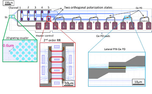
Image courtesy Luceda and Imec
Their simulator is integrated with their layout tool, making it easier to create and then evaluate photonic devices. They claim to have a robust facility for creating custom models; in fact, their simulation technology transcends photonics specifically, lending itself well to “…devices with strong non-linear models, …large networks (1000s of devices) and circuits with a lot [of] strong feedback loops (resonances)” (per Luceda’s Pieter Dumon). They have actually done some electronic circuits (RC networks), but the tool hasn’t been optimized for that; they anticipate co-simulating with a separate electronic simulator.
Mentor/Lumerical join forces (and use PhoeniX Software too)
Mentor Graphics is working with Lumerical to bring photonic simulation closer to the electronics. It’s not integrated simulation; it’s an example of using electronic simulation output as stimulus for photonic simulation. Lumerical’s INTERCONNECT tool handles the photonic simulation, but some of the underlying database elements have been merged so that, for example, you can use Mentor’s Pyxis tool to create a waveform that can serve as a stimulus for INTERCONNECT.
INTERCONNECT can work with a number of different types of models, such as the equivalent of compact models. They support both time- and frequency-domain analysis.
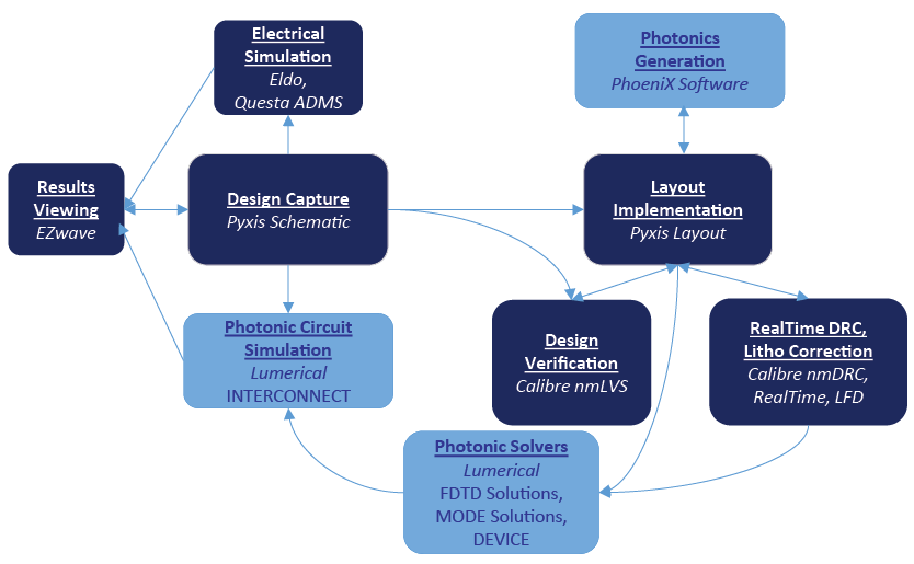
Image courtesy Mentor and Lumerical
They also pull in PDKs from PhoeniX Software. PhoeniX’s focus has been more on cleanroom management and manufacturing, but PDKs are an obvious point where design meets manufacturing.
Synopsys’s RSoft OptSim Circuit does double-duty
Synopsys has a tendency to partner via acquisition. And RSoft was one of them. We’ve looked at a number of Synopsys optical tools in the past, but none of those was specifically about photonics. The RSoft group recently announced their OptSim Circuit for handling integrated electronic/photonic designs.
OptSim Circuit has models of both electronic (drivers, filters, amplifiers, signal generators, and the like) and photonic components, so this is one example where you can do both with a single tool. Alternatively, you can work in a mode where you feed stimulus from, say, SPICE if that’s also a need.
(Click image to enlarge)
Image courtesy Synopsys
That’s the current round-up; we can now add photonics to electronics and MEMS as design tool domains that we need to keep an eye on.
More info:


Are you designing parts of a photonic chip? What do you think about the state of design tools?