


This week we take on a couple of developments in the MRAM world. While much of our more recent MRAM coverage has focused on the newer (and not yet ready for production) SOT (spin-orbit torque) approach, today’s stories are rooted in the more common (and now in production) STT (spin-transfer torque) technology.
Testing the Magnetics
It would probably come as no big surprise that the operation of magnetic RAMs would involve magnetic fields. The nice thing is, however, that, for STT MRAM, all the magnetics are provided electrically in the circuits. (Not so with SOT-MRAM…) So you should be able to test everything without any external magnetic fields, right?
Well, turns out that’s not right. Yes, you can program an MRAM bit using only electrical signals. That’s how it works, after all. But you don’t know what field strength was generated to do that programming; it’s more or less binary: either it programmed or it didn’t, and you don’t know how much margin there was. Ideally, you want to test both the free and pinned (or reference) layers to make sure that everything is, well, sturdy.
If you program using an external field, you can measure the hysteresis curve for both transitions. Because there’s a certain amount of stochastic behavior, however, you likely want to make multiple measurements to confirm repeatability. That could make this a challenge to perform in a timeframe that makes commercial sense for production devices.
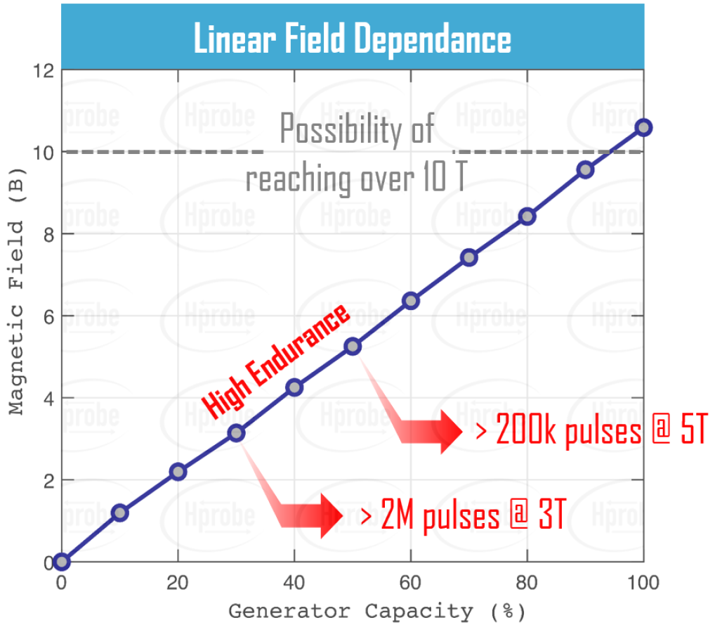
HProbe has built a test head that can apply and sweep a magnetic field quickly enough for production. In fact, they’re now on their second generation, suitable for production of smaller-geometry magnetic tunneling junctions (MTJs). The first-generation device could apply a field of up to a half-Tesla in any direction. The second generation can sweep up to 2 T perpendicular to the die.

(Click to enlarge. Image courtesy HProbe.)
As they crank up the field, they use the resistance through the MTJ as an indication of when the thing switches, and they can then make note of the field strength at that point. They can run the entire curve in less than a second.

(Image courtesy HProbe)
The generator can actually create fields of higher strength – potentially as high as 10 T, although that’s not how they anticipate current devices being tested. A lower sweep is run first to test the free layer; then a higher field is used to test the pinned layer. The pinned layer shouldn’t switch to a stable state; once the external field is removed, it should be restored to the state established (or held) by the synthetic anti-ferromagnetic (SAF) layer.
(Image courtesy HProbe)
Of course, if you go too high, you could alter the SAF layer. So appropriate field targeting is in order – and there is clearly margin to go higher if needed.
To be clear, this solution is intended for use with STT-MRAM technology. I asked if it was also appropriate for SOT-MRAM, and they indicated that, yes, in fact, they’re working with Imec on this, with the ability to generate 200-ps pulses. (Yes, that’s picoseconds.) They’ll need to generate both perpendicular and in-plane fields for that, although they think they’ll require less than 2 T for the in-plane field.
By the way, they note that they can do all of this without requiring any cooling of the magnetic test head or generator.
Can MRAM Contents Survive Soldering?
Meanwhile, there’s been a lurking issue with STT MRAM that, while not deadly, is certainly an inconvenience. MRAM bit cells – especially those with smaller, more aggressive dimensions – can lose their contents if temperatures are too high. This stands to reason, since you’ve got all these nicely aligned dipoles, and, if you shake them around enough thermally, they’re going to randomize to some extent.
It turns out that, when building systems with MRAMs in them, it’s convenient to program the MRAM before it’s assembled onto the board. It also turns out that, at least in some MRAM embodiments, the subsequent step of reflow soldering is hot enough to disrupt the contents to the point of requiring reprogramming before shipping. Programming a die or packaged part with a tester is way easier than programming a part after it’s been soldered down on a board. So, both for hassle and test-time reasons, this extra programming step is annoying.
GlobalFoundries has taken on EverSpin’s MRAM technology, but this remained as a nagging aspect of the technology. So they’ve tweaked the process to ensure that the devices can be reflowed at least 5 times without losing their contents.
How did they do that? That’s a question I put it to Gregg Bartlett, Sr. VP of Engineering, Technology, and Quality. Aaaaand… he wasn’t willing to give away the goods. He did describe the process of finding the solution, though: good old-fashioned materials engineering and design-of-experiments.
The issue is one of maintaining a high gap between the programmed and unprogrammed states of a cell. The more dipoles get randomized, the narrower that gap becomes (until, presumably, if it meets in the middle, you’ve got the average random tunneling current). So they ran a ton of experiments varying materials and parameters until they had it where they wanted it.
Once again, this applies to STT MRAM. I asked whether they had any plans to run SOT MRAM, and the answer was a succinct “No.” He said that getting the STT MRAM material ready for production took a good five years, so that’s what they’re running with. To be clear, it wasn’t a “Hell no! Over my dead body!” thing. It felt to me like the door was left open a crack for further SOT investigation if it gets to the point where it’s ready for prime time. But, until that point, they’re focusing on what they have and what’s working today: STT MRAM.
More info:
Sourcing credit:
Siamak Salimy, CTO, Hprobe
Gregg Bartlett | SVP, Engineering, Technology and Quality, GlobalFoundries


What do you think of Hprobe’s MRAM tester and the MRAM solderability issue discussed by GlobalFoundries?